Liquid crystal display device

Inactive Publication Date: 2009-04-30
MITSUBISHI ELECTRIC CORP
View PDF0 Cites 29 Cited by
  • Summary
  • Abstract
  • Description
  • Claims
  • Application Information

AI Technical Summary

Benefits of technology

[0009]The present invention can provide a liquid crystal display devise that is less susceptible to external electrical fields and capable of reducing the frame area.

Problems solved by technology

However, the IPS mode also has a disadvantage that the alignment state of the liquid crystal and thereby the display state tend to be easily disturbed by external electrical fields.
However, there has been a concern that the infiltration of foreign substances and the difference in expansion rates may cause wrinkles and warping in such a structure in which a conductive film is stuck over the polarizing plate, and thereby decreasing the yield rate.
Furthermore, the conductive material used to connect the housing frame to the polarizing plate occupies some extent of area.
There is a disadvantage that since the conductive material is formed outside of the display area of a liquid crystal display devise, the frame area needs to be increased.
Therefore, there is a disadvantage that the fame area needs to be increased.

Method used


Image

  • Liquid crystal display device
  • Liquid crystal display device
  • Liquid crystal display device

Examples


first embodiment

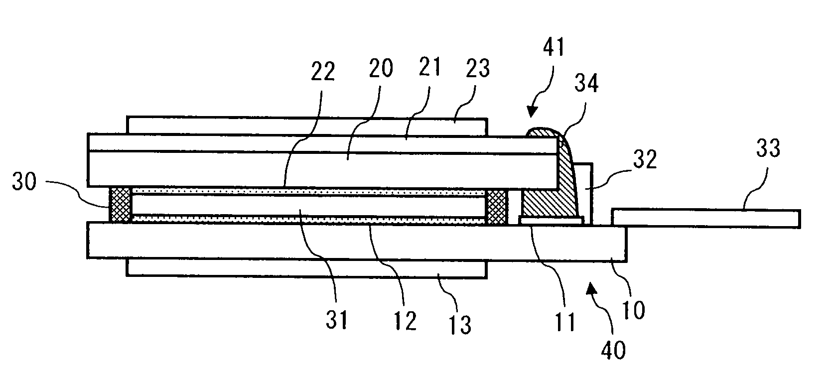
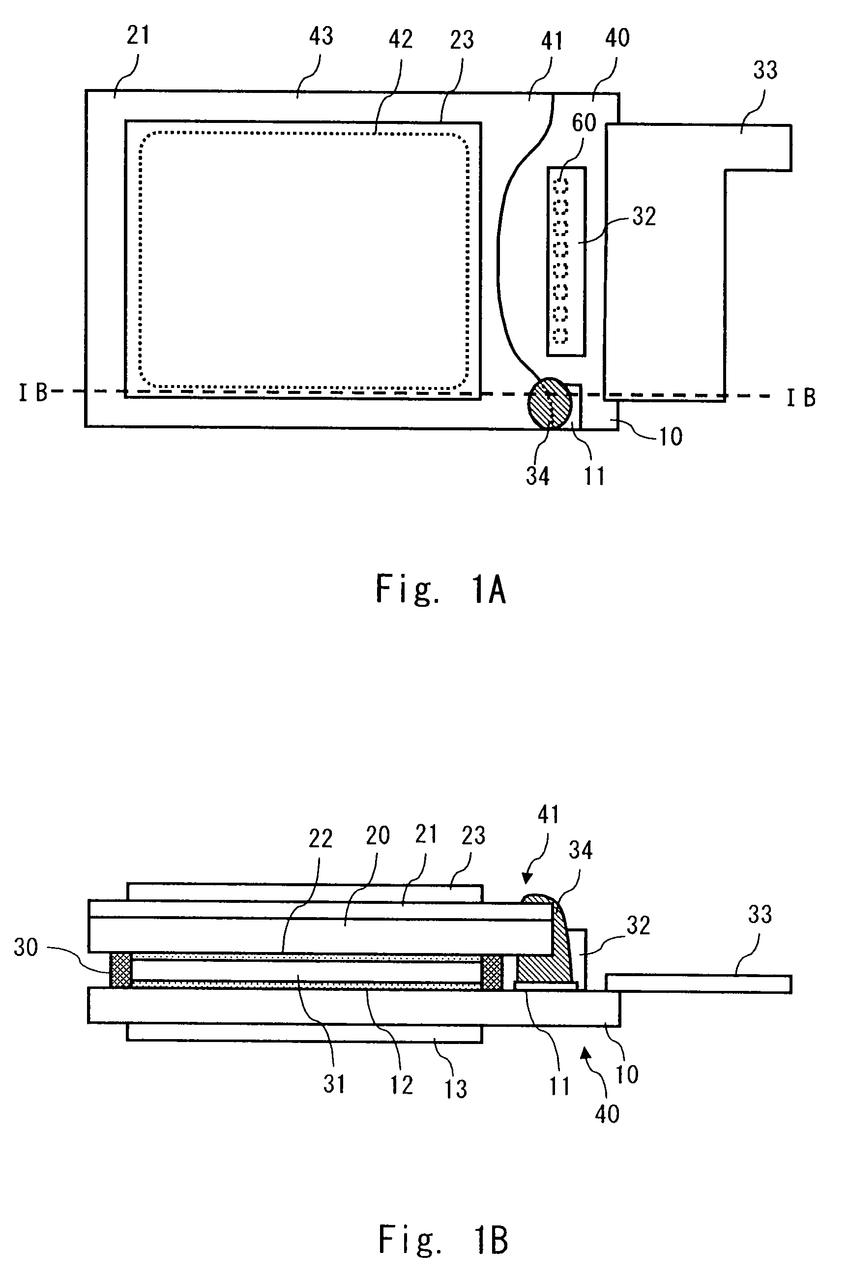
[0020]Firstly, a liquid crystal display devise in accordance with a first embodiment of the present invention is explained hereinafter with reference to FIGS. 1A and 1B. FIG. 1A is a top view showing the structure of a liquid crystal display panel. FIG. 1B is a cross-section taken along the line IB-IB in FIG. 1A. In this example, a liquid crystal display devise of the IPS mode is explained as one example of a liquid crystal display device.

[0021]The liquid crystal display devise includes a liquid crystal display panel, a backlight unit, a driving circuit, and the like. The liquid crystal display panel has such a structure that an array substrate 10 and an opposed substrate 20 are arranged opposite to each other, and a liquid crystal layer 31 is formed in the space enclosed by both substrates and sealing material 30 adhering these substrates. Both of the substrates are maintained so as to have a specific gap between the substrates by spacers.

[0022]Furthermore, among the array substrat...

second embodiment

[0048]This embodiment is different from the first embodiment in that insulating resin is formed in the overhang area 41. Incidentally, other structures are similar to those of the first embodiment, and therefore their explanations are omitted as appropriate.

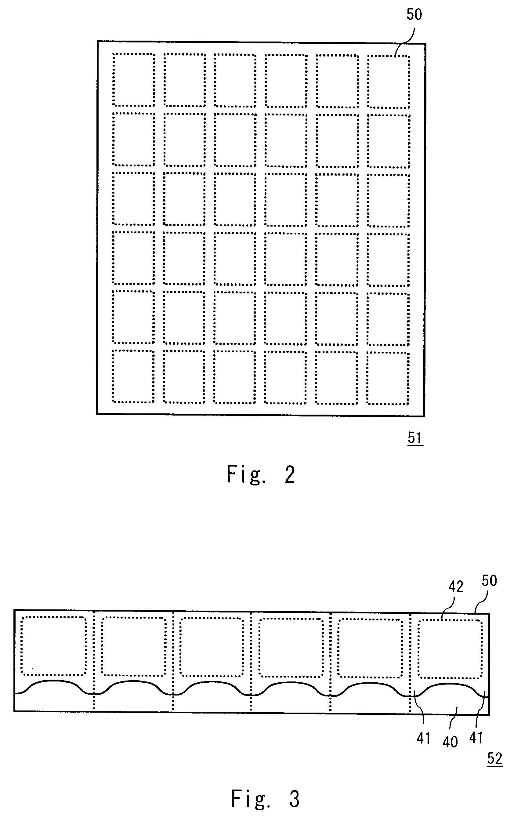
[0049]Insulating resin in accordance with this embodiment of the present invention is explained hereinafter with reference to FIG. 4. FIG. 4 is a top view showing a coating place of insulating resin 36. The insulating resin 36 is, for example, formed from the same material as the sealing material 30. The sealing material 30 is coated or printed along the peripheral portion of the display area 42 such that the sealing material 30 surrounds the display area 42. Incidentally, a liquid crystal filling port 35 is formed at a corner potion on the opposite side to the terminal side in this example. In this embodiment of the present invention, an insulating resin 36 is formed in the overhang area 41. That is, the sealing material 30 is f...

third embodiment

[0050]Although the shape of the ground electrode 11 is not specified in the first embodiment, the ground electrode 11 is formed in a specific shape described below in this embodiment. Incidentally, other structures are similar to those of the first embodiment, and therefore their explanations are omitted as appropriate.

[0051]The shape of the ground electrode 11 in accordance with this embodiment of the present invention is explained hereinafter with reference to FIG. 5. FIG. 5 is a top view showing the structure of the projection area 40 before the driver LSI 32 and the FPC 33 are connected. The driver LSI 32 is connected roughly at the center portion of the projection area 40. Therefore, electrode terminals 60, which will be connected to the bump of the driver LSI 32, are disposed roughly at the center portion of the projection area 40. Furthermore, output lines 61 extending from the display area 42 are also formed in the projection area 40. The electrode terminals 60 are provided ...


PUM


Abstract

In accordance with one aspect of the present invention, a liquid crystal display device having a liquid crystal display panel including a array substrate 10 and an opposed substrate 20 arranged in opposed positions, includes a display area 42, a projection area 40 formed by projecting one edge of the array substrate 10 beyond the opposed substrate on the outside of the display area 42, an electrode terminal 60 formed in the projection area 40, an overhang area 41 formed by overhanging a part of the side edge on the projection area 40 side of the opposed substrate 20, when viewed from the top, toward the side edge of the array substrate located on the projection area 40 side, a conductive film 21 formed on the opposed substrate, and Ag paste 34 formed in the overhang area 41 and electrically connected to the conductive film 21.

Description

BACKGROUND OF THE INVENTION[0001]1. Field of the Invention[0002]The present invention relates to a liquid crystal display device, in particular a liquid crystal display device having an overhang area in a part of the substrate.[0003]2. Description of Related Art[0004]Improvements in the performance of liquid crystal display devises have been remarkably in recent years. In particular, requirements for a wider viewing angle have become higher, and various techniques such as the IPS mode and the VA mode have been proposed and adopted. Especially, the IPS mode excels other techniques in its wider viewing angle. However, the IPS mode also has a disadvantage that the alignment state of the liquid crystal and thereby the display state tend to be easily disturbed by external electrical fields. To solve problem like this, Japanese Unexamined Patent Application Publication No. 10-268783 discloses a technique in which a conductive layer is stuck over the polarizing plate that is in turn stuck ...

Claims


Application Information

Patent Timeline
IPC IPC(8): G02F1/1333G02F1/1343
CPCG02F1/133308G02F2001/133334G02F1/13452G02F1/133334
Inventor MORISHITA, HITOSHI
Owner MITSUBISHI ELECTRIC CORP
Why Eureka
Try Eureka