Electro-optic panel and manufacturing method thereof

a technology of optical panels and manufacturing methods, applied in non-linear optics, identification means, instruments, etc., can solve the problem of limiting the area of occupied areas, and achieve the effect of reducing cost, reducing picture frame area, and not degrading display quality

Active Publication Date: 2006-08-08
SEIKO EPSON CORP
View PDF13 Cites 2 Cited by
  • Summary
  • Abstract
  • Description
  • Claims
  • Application Information

AI Technical Summary

Benefits of technology

[0011]According to the invention, a part of or a whole of the identification pattern with respect to the scanning lines is formed in the dummy pixel area. Since the dummy pixel area does not contribute to image display, display quality will not be degraded, even when the identification pattern is formed therein. Further, since the identification pattern is formed in the area of interest, a picture frame area can be reduced, the electro-optic panel can be miniaturized and lightweight, and the cost can be reduced.
[0012]It is preferred that the dummy pixel area has a first area provided on one end of the respective scanning lines and a second area provided on the other end thereof, and the identification pattern is formed by being divided in the first area and the second area. In this case, since the identification pattern is formed by being divided, the picture frame area can be further reduced, even when the number of scanning lines is large and the digit number of the identification information is large.
[0013]Further, another electro-optic panel according to the invention includes: a plurality of scanning lines; a plurality of data lines; and switching elements disposed in a matrix form so as to correspond to intersections of the scanning lines and the data lines, and respective pixel areas partitioned by the respective scanning lines and the respective data lines have an effective pixel area that contributes to image display and a dummy pixel area that does not contribute to image display. A part of or a whole of an identification pattern representing identification information to identify the respective data lines is formed in the dummy pixel area. According to the invention, since a part of or a whole of the identification pattern with respect to the data lines is formed in the dummy pixel area, a picture frame area can be reduced, the electro-optic panel can be miniaturized and lightweight, and the cost can be reduced.
[0014]It is preferred that the dummy pixel area has a first area provided on one end of the respective data lines and a second area provided on the other end thereof, the identification pattern is formed by being divided in the first area and the second area. In this case, since the identification pattern is formed by being divided, the picture frame area can be further reduced, even when the number of data lines is large and the digit number of the identification information is large.

Problems solved by technology

However, since the identification pattern needs to be of a size that can be checked with a microscope, etc., there is a limit as to how much its occupied area can be reduced.

Method used


Image

  • Electro-optic panel and manufacturing method thereof
  • Electro-optic panel and manufacturing method thereof
  • Electro-optic panel and manufacturing method thereof

Examples


Embodiment Construction

[0034]Exemplary embodiments of the invention are described below by referring to the drawings.

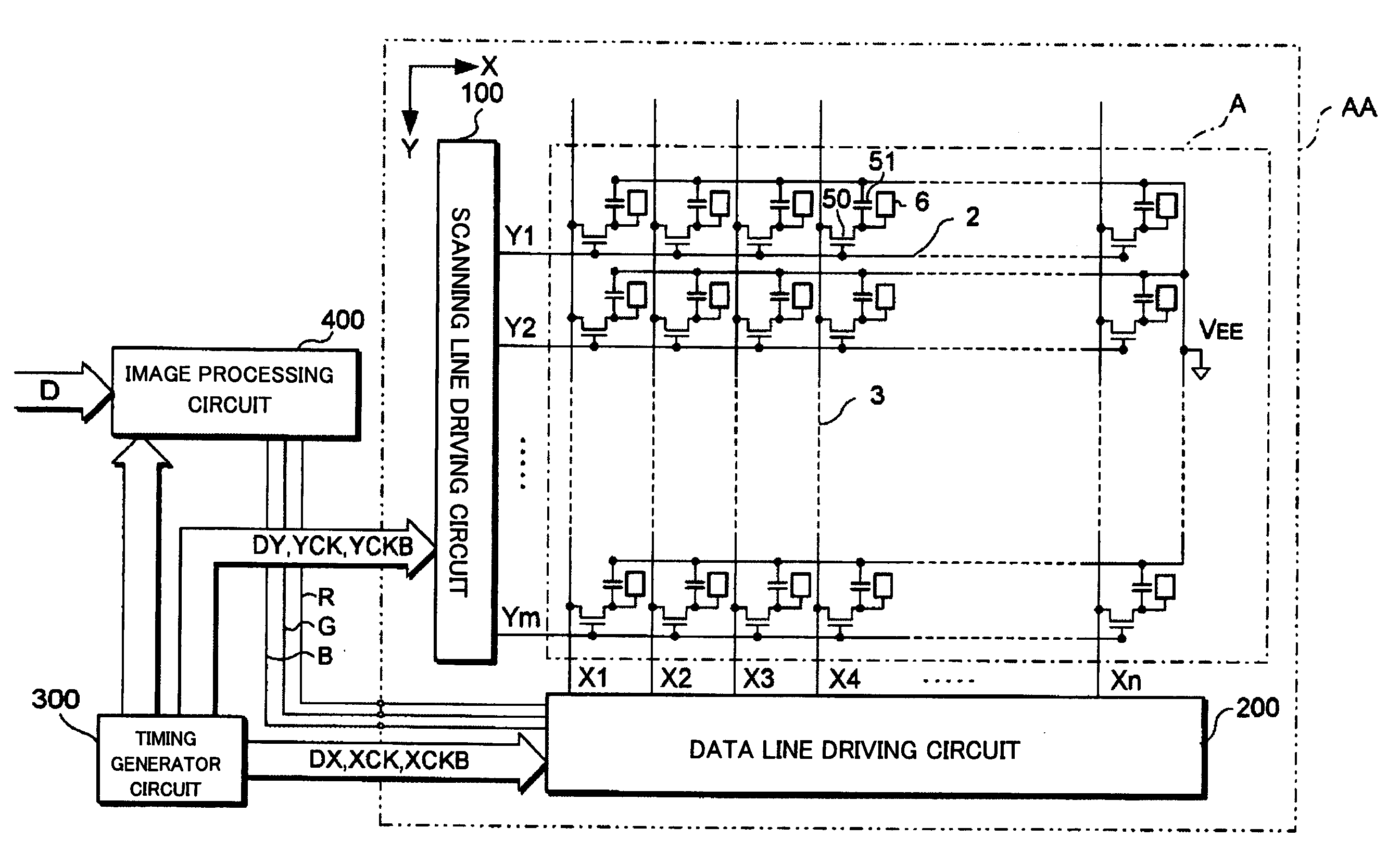
[0035]FIG. 1 is a schematic illustrating an overall structure of a liquid crystal device according to an exemplary embodiment. This liquid crystal device includes a liquid crystal panel AA, a timing generator circuit 300, and an image processing circuit 400. The liquid crystal panel AA has a pixel area A, a scanning line driving circuit 100, and a data line driving circuit 200 on an element substrate thereof.

[0036]Input image data D supplied to the liquid crystal device is, for example, in the form of three-bit parallel. The timing generator circuit 300 generates, in synchronous with the image data D, a Y clock signal YCK, an inversion Y clock signal YCKB, an X clock signal XCK, an inversion X clock signal XCKB, a Y transfer start pulse DY, and an X transfer start pulse DX, and supplies them to the scanning line driving circuit 100 and the data line driving circuit 200. Further, the timing ...


PUM

PropertyMeasurementUnit
thicknessaaaaaaaaaa
angleaaaaaaaaaa
areaaaaaaaaaaa

Abstract

The invention miniaturizes a liquid crystal panel and thus provides a lightweight panel. A TFT provided so as to correspond to intersections of data lines and scanning lines. A dummy pixel area does not contribute to image display, while an effective pixel area contributes to image display. An identification pattern represents a sequence of scanning lines. By forming the identification pattern in the dummy pixel area, the data lines and a scanning line driving circuit can be provided closer to each other, and a picture frame area can be reduced.

Description

BACKGROUND OF THE INVENTION[0001]1. Field of Invention[0002]The present invention relates to an electro-optic panel having a plurality of scanning lines, a plurality of data lines, and switching elements disposed in a matrix form so as to correspond to intersections thereof.[0003]2. Description of Related Art[0004]A related art active matrix type liquid crystal panel mainly includes an element substrate on which switching elements are provided to respective pixel electrodes arranged in a matrix form, a counter substrate on which a color filter, etc., is formed, and liquid crystal filled between these substrates. In such a structure, applying a scan signal to the switching element via the scanning line, the switching element of interest is turned in a conduction state. In this conduction state, applying an image signal to the pixel electrode via the data line, predetermined electric charge is stored in a liquid crystal layer between the pixel electrode of interest and a counter elect...

Claims


Application Information

Patent Timeline
Patent Type & Authority Patents(United States)
IPC IPC(8): G02F1/1343G02F1/13G02F1/1362G02F1/1368G09F9/00
CPCG02F1/134309G02F1/136286G02F1/1343
Inventor FUJITA, SHIN
Owner SEIKO EPSON CORP
Why Eureka
Try Eureka