Display unit having sealing structure and manufacturing method of same

a technology of sealing structure and display unit, which is applied in the direction of discharge tube luminescnet screen, identification means, instruments, etc., can solve the problems of inability to completely prevent the intrusion of moisture through adhesive or the like into the inside of the sealing unit, the deterioration of the illumination, and the inability to completely prevent the manufacturing process and cost of the product. achieve the effect of improving reliability and reducing the frame area

Active Publication Date: 2007-09-25
JOLED INC
View PDF15 Cites 2 Cited by
  • Summary
  • Abstract
  • Description
  • Claims
  • Application Information

AI Technical Summary

Benefits of technology

[0010]In light of the foregoing, it is an object of the invention to provide a display unit which can improve reliability and reduce a frame area by forming a protective film over an entire display area in a uniform film thickness and its manufacturing method.

Problems solved by technology

There is the possibility that in the organic light emitting display, an area which emits no light (dark spot) is generated and luminance deteriorates due to intrusion of moisture, oxygen and the like into the organic light emitting device.
This sealing method by using such sealing can, however, has problems in its manufacturing process and its cost.
In addition, there is the possibility that intrusion of the moisture through the adhesive or the like into inside of the sealing can cannot be completely prevented.
However, in the case where sealing is made by covering the organic light emitting device by the thin film, there is a problem that a part which is not covered with the thin film is generated due to exfoliation of the thin film caused by residual stress and low step coverage.
Therefore, in this case, it is difficult to completely block moisture, oxygen and the like from intruding into the organic light emitting device.
However, since masking causes limitation of active agent and separation of plasma, a film thickness distribution of the protective film at mask edge matters in general deposition processes such as sputter deposition, CVD (chemical vapor deposition) and the like, particularly in CVD.
In addition, there is the possibility that a distance between the slanting end face of the protective film and the organic light emitting device becomes short, leading to easy intrusion of moisture and the like, and then causing lowering of reliability of the organic light emitting device.
However, making the mask thickness thin causes lowering of adhesion of the mask.
In particular, in some cases of the CVD process which has wraparound, the protective film gets into the clearance between the mask and a substrate or the external connection terminal, and reliability of the external connection terminal is ruined.

Method used


Image

  • Display unit having sealing structure and manufacturing method of same
  • Display unit having sealing structure and manufacturing method of same
  • Display unit having sealing structure and manufacturing method of same

Examples


example 1

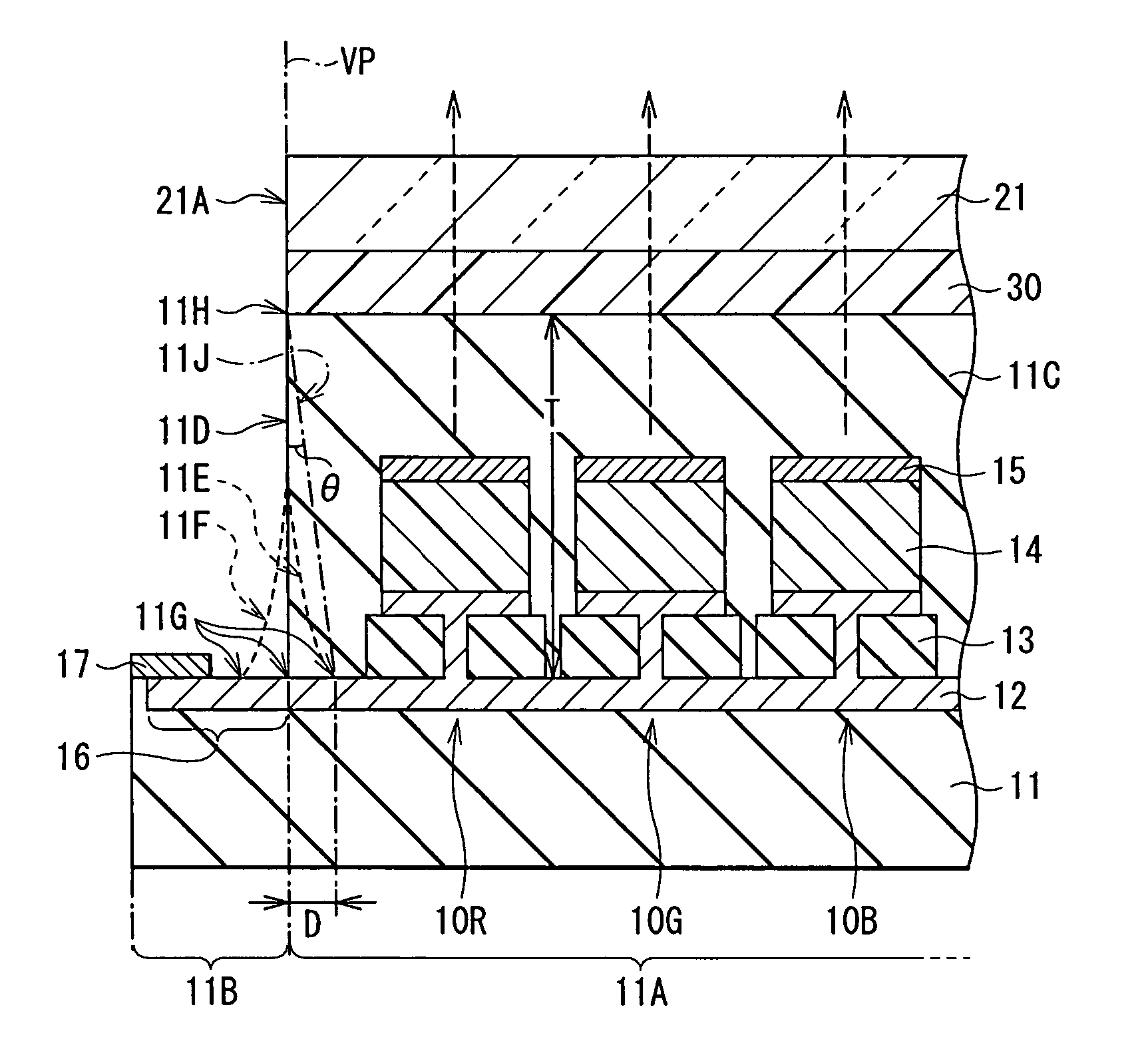
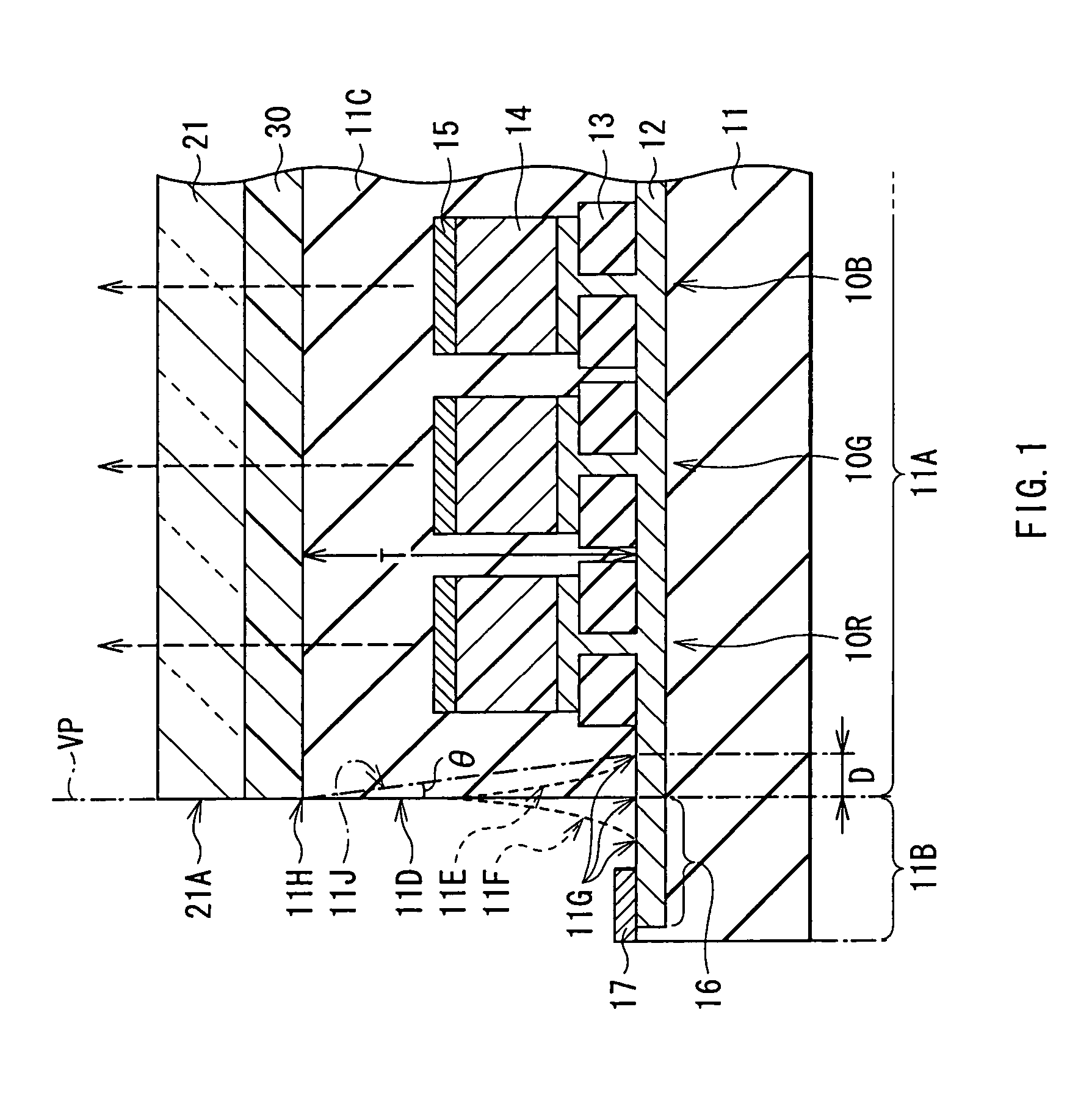
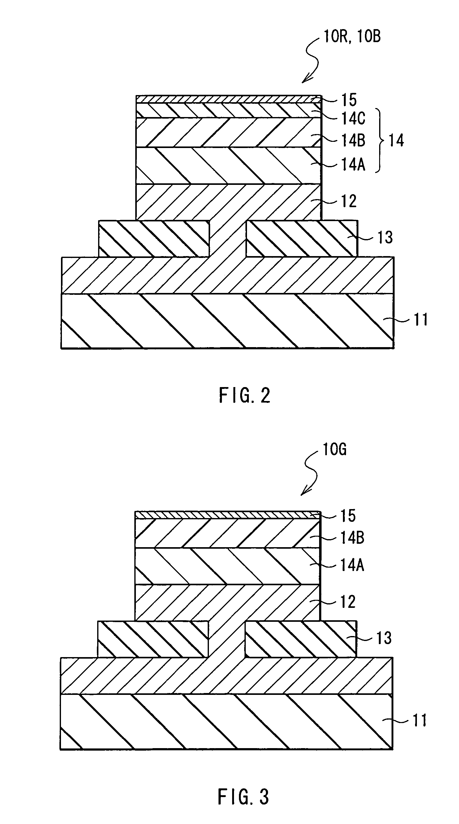
[0057]In the driving substrate 11, the display area 11A was formed and the external connection area 11B was formed adjacently to the display area 11A in the same manner as in the foregoing embodiment, except that the organic light emitting device 10G was only provided. Further, the protective film 11C made of SiNx in its set film thickness of 2 μm was formed over the whole face of the driving substrate 11. As conditions for deposition, a plasma CVD unit with 13.56 MHz was used, SiH4, NH3, and N2 were supplied in respective flows of 100 sccm, 400 sccm, and 2,000 sccm, and 60 Pa and 100W were applied. After that, the sealing substrate 21 was arranged in the area corresponding to the display area 11A of the driving substrate 11, the driving substrate 11 and the sealing substrate 21 were bonded with the adhesive layer 30 in between, and the end face 11D of the protective film 11C was formed by anisotropic etching using the sealing substrate 21 as a mask. In such anisotropic etching, a R...

example 2

[0058]A display unit was produced in the same manner as in Example 1, except that a radical source was used in anisotropic etching, and CF4 was radicalized. As the radical source, USC made by ULVAC was used.

[0059]As a comparative example in relation to Examples 1 and 2, a display unit was produced in the same manner as in Example 1, except that an external connection area 111B was covered with a mask 118 in a thickness of 1 mm made of Al2O, a protective film 111C was formed in a display area 111A, and then the protective film 111C and a sealing substrate 121 were bonded with an adhesive layer 130 in between, as shown in FIG. 8. Then, the mask 118 was formed so that an opening 118A becomes the same size as that of the sealing substrate 121, in order to obtain the external connection area 111B of the comparative example with the same size as that of the external connection area 11B of Examples 1 and 2. In FIG. 8, components corresponding to those in FIG. 1 are applied with symbols whi...


PUM

PropertyMeasurementUnit
distanceaaaaaaaaaa
thicknessaaaaaaaaaa
thicknessaaaaaaaaaa

Abstract

The invention provides a display unit which can improve reliability and reduce a frame area by forming a protective film in a uniform film thickness over an entire display area, and its manufacturing method. An end face of the protective film is formed along a vertical plane including a corresponding end face of a sealing substrate. The end face of the protective film is formed into an approximately vertical cross section in the position of the end face of the sealing substrate, and the entire display area is covered with the protective film in a uniform film thickness. It is preferable that a distance between a lower end of the end face and the vertical plane is set to 2 mm or less. It is preferable that the end face of the protective film is formed by anisotropic etching using the sealing substrate as a mask, after the protective film is formed over a whole face of a driving substrate.

Description

BACKGROUND OF THE INVENTION[0001]1. Field of the Invention[0002]The present invention relates to a display unit having a complete solid sealing structure wherein a driving substrate provided with a display area and a sealing substrate are bonded with an adhesive layer in between and its manufacturing method, and more particularly such a display unit wherein organic light emitting device is provided in its display area and its manufacturing method.[0003]2. Description of the Related Art[0004]As a display unit instead of a liquid crystal display, an organic light emitting display which uses organic light emitting device has been noted. The organic light emitting display has characteristics that its visual field angle is wide and its power consumption is low since it is a self-light emitting type display. The organic light emitting display is also thought of as a display having sufficient response to high-definition high-speed video signals, and is under development toward the practica...

Claims


Application Information

Patent Timeline
Patent Type & Authority Patents(United States)
IPC IPC(8): H05B33/04G09F9/00H01L27/32H01L51/50H01L51/52H01L51/56H05B33/10H05B33/14
CPCH01L51/56H01L51/5237H01L27/3211H01L27/3281Y10S428/917H01L2251/5315H10K59/35H10K59/17H10K50/841H10K50/844H10K50/8426H10K2102/3026H10K71/00H05B33/04
Inventor MORI, TAKAOENDA, MASASHI
Owner JOLED INC
Why Eureka
Try Eureka