
Plasma display panel and deposition apparatus used in the manufacturing thereof

a technology of deposition apparatus and display panel, which is applied in the manufacture of electrode systems, cold cathode manufacturing, electric discharge tube/lamp manufacture, etc., can solve the problems of difficult to realize a stable display, and achieve the effect of not affecting the luminosity of the variation between cells

Inactive Publication Date: 2009-06-11
FUJITSU HITACHI PLASMA DISPLAY LTD
View PDF4 Cites 0 Cited by
  • Summary
  • Abstract
  • Description
  • Claims
  • Application Information

AI Technical Summary

Benefits of technology

[0013]A first object of the present invention is to provide a plasma display panel in which the peak value of the discharge current is low and variation in luminosity between cells does not stand out. A second object is to provide a method and apparatus for manufacturing suited to the mass production of a plasma display panel that achieves the first object.
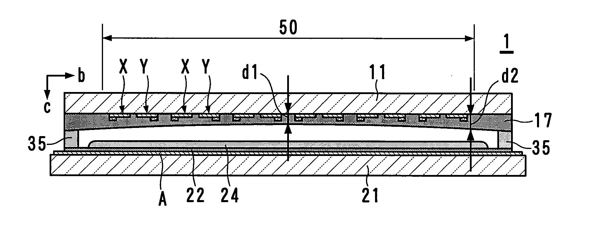
[0015]The discharge starting voltage for cells where the dielectric layer is thick is higher than the discharge starting voltage for cells where the dielectric layer is thin, and therefore with a structure in which the thickness of the dielectric layer differs depending on the position in the screen, the variation in the discharge starting period between cells is much more prominent than as compared to a structure in which the thickness of the dielectric layer is consistent across the entire screen. The variation in the discharge starting period relaxes the concentration of the discharge current. When the same voltage is applied to all cells, cells with a low discharge starting voltage (in other words, cells in the central portions of the screen) emit a stronger discharge than cells with a high discharge starting voltage (in other words, cells in the peripheral portions of the screen), and thus the luminance thereof is high. To put it differently, a distributed luminosity corresponding to the thickness of the dielectric layer arises at the time of display. It is basically desirable for the luminosity to be equal throughout the screen, but because viewers of displays frequently look at the central portion of the screen, a distributed luminosity in which the central portion of the screen has a high luminosity that decreases toward the periphery will not stand out.

Problems solved by technology

Furthermore, because the discharge properties of the cells differ significantly between the two ends, the permissible range (margin) of the driving voltage is narrow, and thus it is difficult to realize a stable display.

Method used


Image

  • Plasma display panel and deposition apparatus used in the manufacturing thereof
  • Plasma display panel and deposition apparatus used in the manufacturing thereof
  • Plasma display panel and deposition apparatus used in the manufacturing thereof

Examples


Embodiment Construction

[0023]A surface-discharge type plasma display panel in which both of first and second electrodes for achieving display discharge are covered by a dielectric layer is suited to the implementation of the present invention.

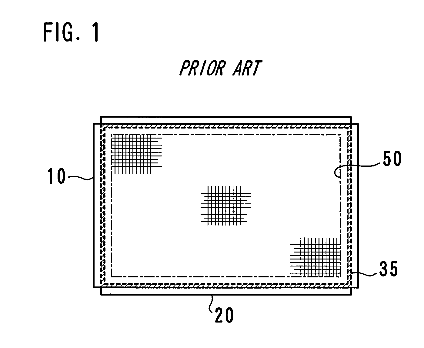
[0024]As shown in FIG. 1, the plasma display panel has a front panel 10, a rear panel 20, and a screen 50 configured of cells (light-emitting elements) arranged horizontally and vertically and a discharge gas (not shown). If the screen size is, for example, 42 inches on the diagonal, the plasma display panel is approximately 994 mm by 585 mm. The front panel 10 and the rear panel 20 are members in which multiple layers including electrodes are affixed to an approximately 3 mm-thick glass substrate that is larger than the screen 50. The front panel 10 and the rear panel 20 are arranged opposite each another so as to overlap, and are connected to each another by sealant 35 in a frame shape when viewed from the front disposed in the peripheral portions of the area where...


PUM

PropertyMeasurementUnit
sizeaaaaaaaaaa
sizeaaaaaaaaaa
sizeaaaaaaaaaa

Abstract

A plasma display panel has a screen (50) composed of a plurality of cells and a dielectric layer (17) across the entirety of the screen, and each cell includes a discharge space (31) filled with a discharge gas, a pair of electrodes (X, Y) for causing discharge in the discharge space (31), and a dielectric that is part of the dielectric layer (17) and that is interposed between the discharge space (31) and the electrodes (X, Y). The dielectric layer (17) has such a distribution of thickness that the dielectric layer is thinnest at the central portion of the screen and is gradually growing from the central portion of the screen toward the peripheral portions of the screen. The distribution of thickness in the dielectric layer makes the variation in the discharge delay between cells prominent, thereby relaxing the concentration of the discharge current.

Description

TECHNICAL FIELD[0001]The present invention relates to a plasma display panel having a dielectric layer that covers electrodes, a method for manufacturing the plasma display panel, and a deposition apparatus used in the manufacturing.BACKGROUND ART[0002]AC-type plasma display panels, which are useful for displaying color images, have a dielectric layer that covers electrodes. The dielectric layer is interposed between the electrodes and a discharge space, and the dielectric layer is charged with a charge called a “wall charge”. AC-type plasma display panels use a wall voltage generated through the charging of the wall charge in their display.[0003]For display images, an operation for writing data in a line-sequential scanning format (addressing) is performed, whereby the cells to be illuminated among the cells arranged on the screen in a matrix are given a higher wall voltage than the wall voltage of the other cells. After this, an operation for maintaining the illumination (sustain)...

Claims


Application Information

Patent Timeline
Patent Type & Authority Applications(United States)
IPC IPC(8): H01J61/00H01J9/00H01J11/12H01J11/38
CPCC23C16/45565C23C16/5096H01J11/38H01J11/12H01J9/02
Inventor NANTO, TOSHIYUKI
Owner FUJITSU HITACHI PLASMA DISPLAY LTD
Learn More