High-voltage MOS transistor

a high-voltage mos, transistor technology, applied in the direction of basic electric elements, electrical equipment, semiconductor devices, etc., can solve the problems of short actual service life of the transistor and the inability to sacrifice the driving capacity of the transistor itself, so as to achieve the effect of reducing the peak value and sufficient lifetime of the hot carrier

Inactive Publication Date: 2005-12-13
LAPIS SEMICON CO LTD
View PDF2 Cites 1 Cited by
  • Summary
  • Abstract
  • Description
  • Claims
  • Application Information

AI Technical Summary

Benefits of technology

[0022]That is, the invention has been developed with an eye on a lifetime of hot carriers, thereby finding out an optimum overlapping width of the gate electrode on the first diffusion layer (lightly doped diffusion layer) in the drain region that ensures a sufficient lifetime of the hot carriers.
[0023]According to a first aspect of the invention, by overlaying the gate electrode on at least the first diffusion layer in the drain region (overlapping each other) in, a plan view, the peak value of an impact ionization as well as an electric field, in the boundary region between the gate electrode and the first diffusion layer, can be spread out within a range of such overlapping (an overlapping region), so that the peak values can be rendered lower accordingly.

Problems solved by technology

That is, it means that an actual service life of a transistor is short.
With such methods as described, however, there has arisen a problem that the driving capacity of the transistor itself had to be inevitably sacrificed due to an increase in diffusion resistance of the source / drain, and channel resistance.

Method used


Image

  • High-voltage MOS transistor
  • High-voltage MOS transistor
  • High-voltage MOS transistor

Examples


first embodiment

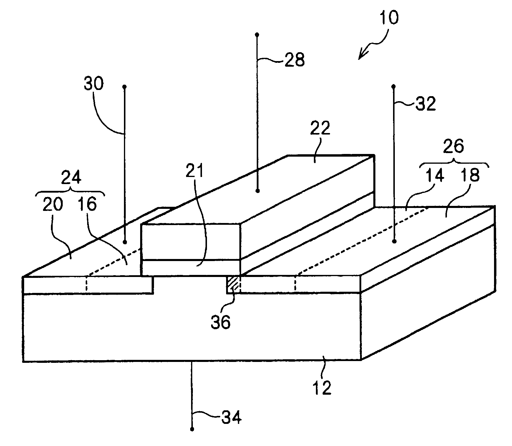
[0037]FIGS. 1 and 2 show an n-channel high-voltage MOS transistor 10 according to the invention. The n-channel high-voltage MOS transistor 10 comprises a p-type silicon semiconductor substrate 12, a pair of symmetrical n-type regions (lightly doped n-type diffusion layers 14, 16, and heavily doped n-type diffusion layers 18, 20 to be described later), disposed in close proximity of a surface (upper surface) of the substrate 12, a gate insulation film 21 provided on the surface of the substrate 12, between the n-type regions, and a gate electrode 22 provided on top of the gate insulation film 21.

[0038]The gate electrode 22 on the p-type silicon semiconductor substrate 12 is made of polysilicon, and the gate insulation film 21 is made up of a gate oxide film.

[0039]With the present embodiment, the gate insulation film 21 is first formed, and subsequently, a mask for forming the lightly doped n-type diffusion layers 14, 16 as first diffusion layers is formed on the gate insulation film ...

second embodiment

[0058]The second embodiment is characterized in that there is provided a relative difference in dopant dose between a surface layer side of a lightly doped n-type diffusion layer 14 and an intermediate layer region thereof.

[0059]More specifically, FIG. 7 is a dose distribution profile at the sectional face taken on line VII—VII of FIG. 6, and as shown in FIG. 7, the dopant dose gradually increases from the surface layer side of the lightly doped n-type diffusion layer 14 towards a p-type silicon semiconductor substrate 12, and reaches a peak in the intermediate layer region, declining towards the back side thereof, that is, on the p-type silicon semiconductor substrate 12 side.

[0060]It is shown that the dopant dose on the surface layer side is 4 E 17 cm−3, and the dopant dose of the intermediate layer (at a position 0.12 μm from the surface layer face), reaching the peak, is 7 E 17 cm−3. In forming the lightly doped n-type diffusion layer 14 described above, a highly doped region is...


PUM


Abstract

A high-voltage MOS transistor capable of lowering the maximum substrate current without sacrificing the driving capacity of the transistor itself, and ensuring an acceptable lifetime of hot carriers is provided. By providing an overlapping region in a boundary region between a gate electrode and a lightly doped n-type diffusion layer of a drain electrode, it becomes possible to increase by about 50% a dopant dose of the lightly doped n-type diffusion layer, having effects on the so-called transistor characteristic of the n-channel high-voltage MOS transistor described above. Furthermore, by setting an overlapping amount to not less than 0.5 μm, it becomes possible to create a stable region with maximum substrate current (Isub max.) at not larger than 5 μA/μm.

Description

BACKGROUND OF THE INVENTION[0001]1. Field of the Invention[0002]The present invention relates to a high-voltage MOS transistor comprising a semiconductor substrate, a gate electrode disposed on the semiconductor substrate with an insulation film interposed therebetween, a pair of first diffusion layers formed on a surface layer side of the semiconductor substrate and disposed apart from each other by a predetermined distance under the gate electrode, and a pair of second diffusion layers, each adjacent to the side of the respective first diffusion layers, facing away from the gate electrode, and having a dopant dose higher than that for the first diffusion layers, wherein a source region is made up of one of the first diffusion layers, and one of the second diffusion layers adjacent to the one of the first diffusion layers and a drain region is made up of the other of the first diffusion layers, and the other of the second diffusion layers, adjacent to the other of the first diffusi...

Claims


Application Information

Patent Timeline
Patent Type & Authority Patents(United States)
IPC IPC(8): H01L21/336H01L21/265H01L29/08H01L29/78
CPCH01L29/0847H01L29/7835H01L29/7836
Inventor MAEKAWA, HISAYUKI
Owner LAPIS SEMICON CO LTD
Why Eureka
Try Eureka