Power semiconductor module

a technology of semiconductor modules and semiconductor components, applied in semiconductor devices, semiconductor/solid-state device details, electrical apparatus, etc., can solve the problems of increasing temperature, generating a large amount of heat, and generating power loss, and achieves high reliability power, sufficient life, and no thermal cycling of defects

Inactive Publication Date: 2010-05-06
TOYOTA JIDOSHA KK +1
View PDF8 Cites 21 Cited by
  • Summary
  • Abstract
  • Description
  • Claims
  • Application Information

AI Technical Summary

Benefits of technology

[0079]According to the present invention, it is possible to provide a highly reliable power semiconductor module in which deficiencies such as cracking and peeling are not caused through thermal cyclings.
[0080]In particular, according to the present invention, it is possible to provide a power semiconductor module having a sufficient lifetime even under thermal cyclings having a large difference in temperature such as from −40 to 200° C.

Problems solved by technology

Thus, a power loss (a steady loss and a switching loss) is generated, generating a large amount of heat and raising the temperature.
In power semiconductor modules, solder bonding sections at the two positions are weakest; thus, deficiencies often generated when a thermal cycling test is employed are caused in the solder bonding sections at the two positions.
Specifically, if the temperature for the second soldering is higher than the melting point of the solder material used in the first soldering, the portion obtained by the first soldering will be melted at the time of the second soldering, resulting in misalignment or inclination of the bonded components, or other deficiencies.
However, the melting point of an Sn based soldering material may only be varied within a narrow range around 220° C. Thus, it is difficult to apply an Sn material to the first and second soldering processes.
Moreover, the tensile strength thereof decreases remarkably at about 200° C. For this reason, for the next-generation power semiconductor elements which generate heat over 200° C., it is difficult to use an Sn based material is used as a bonding material in practice.
However, according to this document, only the strength of the insulator is evaluated, and evaluation is not performed of a module in which the insulator is soldered to another member such as a power semiconductor or a radiator plate.

Method used


Image

  • Power semiconductor module
  • Power semiconductor module
  • Power semiconductor module

Examples


example 1

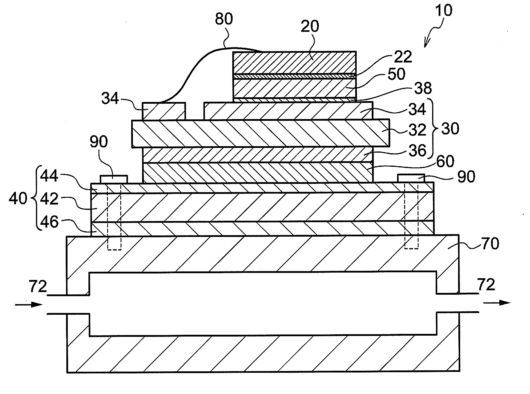
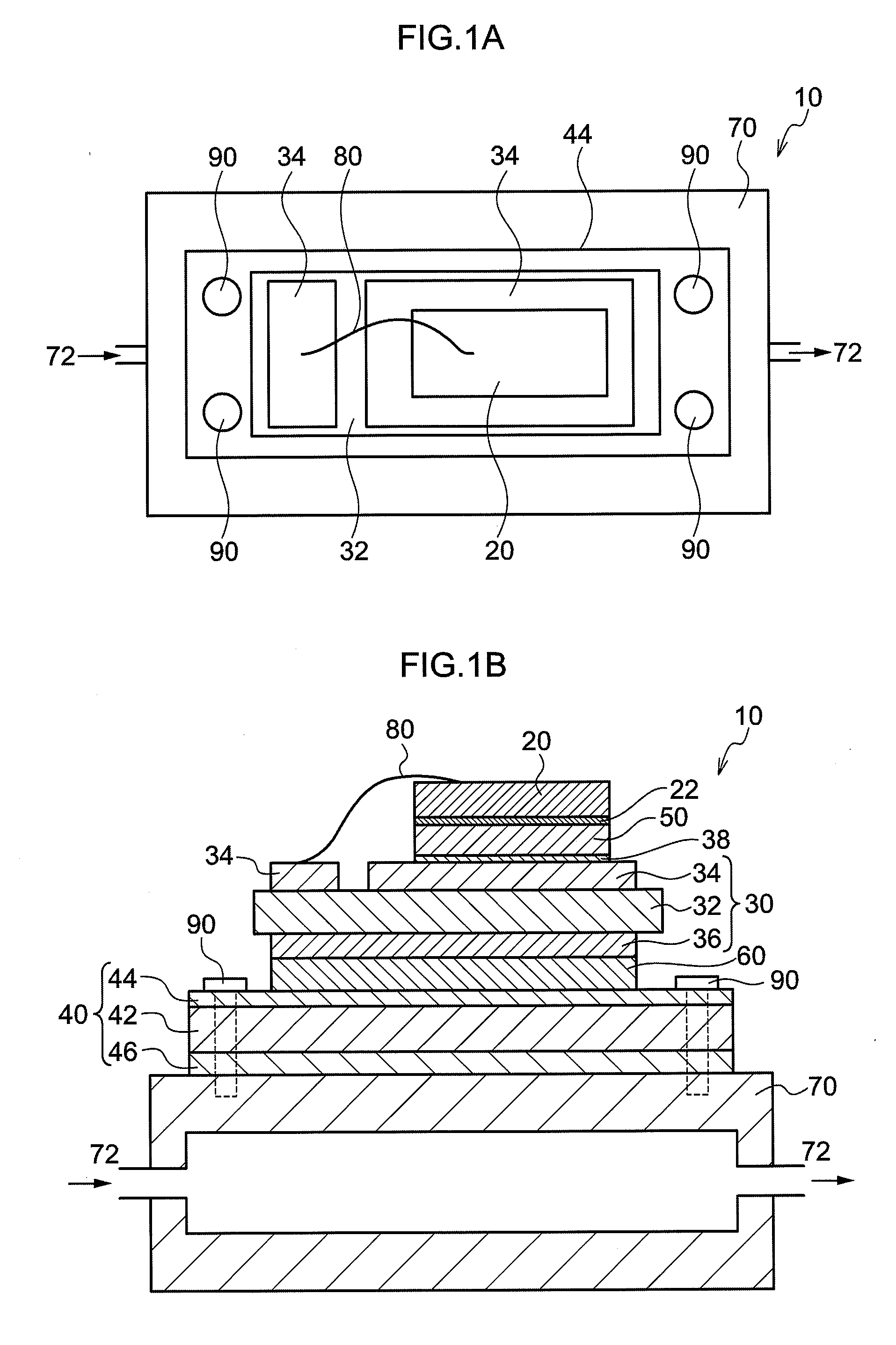
[0279]FIG. 1 shows the structure of a power semiconductor module of the present example.

[0280]

[0281]A power semiconductor element 20 was prepared in 12 mm×9 mm in size, by using SiC (coefficient of thermal expansion: 3 ppm / ° C.). A Ni layer 22 was formed on an outermost surface thereof by sputtering. An Au layer (not illustrated) was formed on the surface of the Ni layer 22 by sputtering.

[0282]

[0283]As an insulating part 30, a laminated body of a Cu layer 34 / SiNx layer 32 / Cu layer 36 was formed.

[0284]First, SiNx having 0.32 mm in thickness was prepared, and the Cu layers 34 and 36 having 0.05 mm in thickness were attached to both surfaces of this SiNx by brazing, so as to form a laminate-1.

[0285]Laminates-2, -3 and -4 were formed in the same manner, except that the thickness of the Cu layers 34 and 36 were changed to 0.1 mm, 0.15 mm or 0.3 mm, respectively. At the both surfaces of the SiNx, the thicknesses of the Cu layers were made equal to each other.

[0286]Insulating part laminate...

example 2

[0310]An evaluating test body-1 was produced, in which a power semiconductor element and an insulating part were bonded to each other by a Bi based solder material, as shown in FIG. 8.

[0311]

[0312]The power semiconductor element 20 was prepared in 12 mm×9 mm in size, by using SiC (coefficient of thermal expansion: 3 ppm / ° C.). A Cu layer 22 was formed on an outermost surface thereof by sputtering.

[0313]

[0314]The laminate-2 (the layer thickness of the Cu layer: 0.1 mm) of the insulating part in Example 1 was prepared.

[0315]

[0316]A pure Bi substance was cut into a thickness of 150 to 220 μm. An oxide film covering the surface of the cut pure Bi substance was removed by use of polishing and washing with an acid.

[0317]The Cu layer 22 of the power semiconductor element 20 prepared as described above and the Cu layer 34 of the insulating part 30 were arranged to be opposed to each other. In the state where the pure Bi substance layer was sandwiched therebetween, a reflow method in the atmo...

example 3

[0324]An evaluating test body-2 was produced in the same manner as in Example 2, except that the pure Bi substance as a bonding material was replaced by a material in which 1% by mass of Cu was added to Bi.

[0325]The resultant evaluating test body-2 was tested in the same thermal cycling test as in Example 2. As a result, a reaction product was not observed at the interfaces of the bonding sections. Neither voids nor cracks were recognized. Accordingly, it was verified that the evaluating test body-2 was highly reliable even through the thermal cyclings under the severe conditions.


PUM


Abstract

Provided is a power semiconductor module in which two components are bonded by a Bi based solder material. A Cu layer is provided on the surfaces thereof to be bonded by the Bi based solder material on the two-component. Two components, i.e., the components to be bonded, are a combination of a semiconductor element and an insulating part, or a combination of an insulating part and a radiator plate. The insulating part is composed of a Cu/SiNx/Cu laminated body.

Description

TECHNICAL FIELD[0001]The present invention relates to a power semiconductor module.BACKGROUND ART[0002]Usually, power semiconductor modules have a structure in which an insulator is provided to a power semiconductor so as to insulate the power semiconductor electrically from a current conducting section. This power semiconductor and the insulator are bonded to each other by a solder or the like.[0003]Power semiconductor modules are each provided with a radiator plate in order to radiate heat generated from their semiconductor element effectively or dissipate the heat temporarily. This radiator plate and the insulator are bonded to each other by a solder. Accordingly, in general, in a power semiconductor modules, bonding with a solder is performed at two positions: a position between a semiconductor element and an insulator; and a position between an insulator and a radiator plate.[0004]In power semiconductor modules, a large electric current flows into a power semiconductor element....

Claims


Application Information

Patent Timeline
Patent Type & Authority Applications(United States)
IPC IPC(8): H01L23/488H01L29/12
CPCH01L2224/29111H01L23/3735H01L23/473H01L24/32H01L25/072H01L24/33H01L24/45H01L24/83H01L2224/45124H01L2224/48091H01L2224/48227H01L2224/73265H01L2224/838H01L2924/01005H01L2924/01014H01L2924/01015H01L2924/01018H01L2924/01027H01L2924/01029H01L2924/0103H01L2924/01032H01L2924/01033H01L2924/01042H01L2924/01047H01L2924/0105H01L2924/01051H01L2924/01078H01L2924/01079H01L2924/01082H01L2924/01322H01L2224/32225H01L2924/0132H01L24/29H01L24/48H01L2224/48472H01L2224/83805H01L2924/01006H01L2924/01019H01L2924/014H01L2924/0133H01L2224/83447H01L2924/1579H01L2924/01028H01L2224/29113H01L2924/351H01L2924/00011H01L24/73H01L2924/00014H01L2924/00H01L2924/00012H01L2924/01013H01L2924/01025H01L2924/01083H01L2924/3512H01L2924/00015H01L2224/83205H01L2224/2612
Inventor YAGI, YUJIYAMADA, YASUSHINAKAGAWA, IKUOATSUMI, TAKASHISHIRAI, MIKIOOHNUMA, IKUOISHIDA, KIYOHITOTAKAKU, YOSHIKAZU
Owner TOYOTA JIDOSHA KK
Why Eureka
Try Eureka