
Memory Circuit with Decoupled Read and Write Bit Lines and Improved Write Stability

a memory circuit and write bit technology, applied in the field of electronic memory circuits, can solve the problems of significant threshold voltage fluctuation and deterioration of static random access memory (sram) stability, and achieve the effect of improving write stability in memories

Inactive Publication Date: 2009-06-11
GLOBALFOUNDRIES INC
View PDF3 Cites 0 Cited by
  • Summary
  • Abstract
  • Description
  • Claims
  • Application Information

AI Technical Summary

Benefits of technology

[0008]Principles of the present invention provide techniques for improving WRITE stability in memories with decoupled READ and WRITE bit lines. In one aspect, an exemplary memory circuit includes a plurality of cells that form rows and columns. The circuit further includes a retained data latch, a latch for new data (also referred to herein as a new data latch), and control circuitry operatively coupled to the cells, the retained data latch, and the new data latch. The control circuitry is configured to write data during a WRITE operation. In a first cycle, data associated with all cells in a given one of the rows that is to be written to is read into the retained data latch, and new data to delay the WRITE operation for a cycle is stored into the new data latch. In an immediately subsequent second cycle, the read data from the retained data latch is written back to those of the cells that are in a half-select condition, and the new data from the new data latch is written to those of the cells that are in a full-select condition.

Problems solved by technology

As device size shrinks down aggressively in advanced very large scale integration (VLSI) technology, increased process variation causes significant amounts of threshold voltage fluctuation.
As a result, stability of static random access memory (SRAM) deteriorates due to the large threshold voltage mismatch between two neighboring transistors in a cell.

Method used


Image

  • Memory Circuit with Decoupled Read and Write Bit Lines and Improved Write Stability
  • Memory Circuit with Decoupled Read and Write Bit Lines and Improved Write Stability
  • Memory Circuit with Decoupled Read and Write Bit Lines and Improved Write Stability

Examples


Embodiment Construction

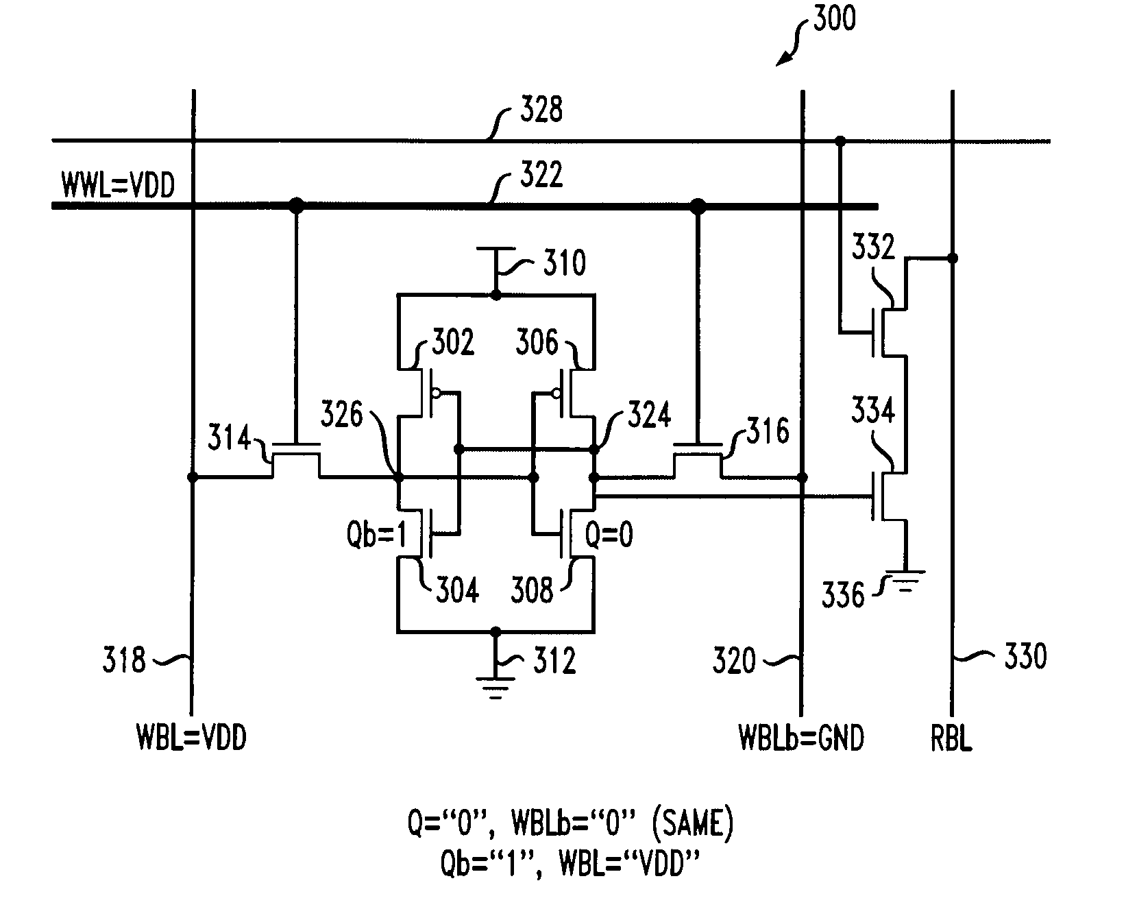
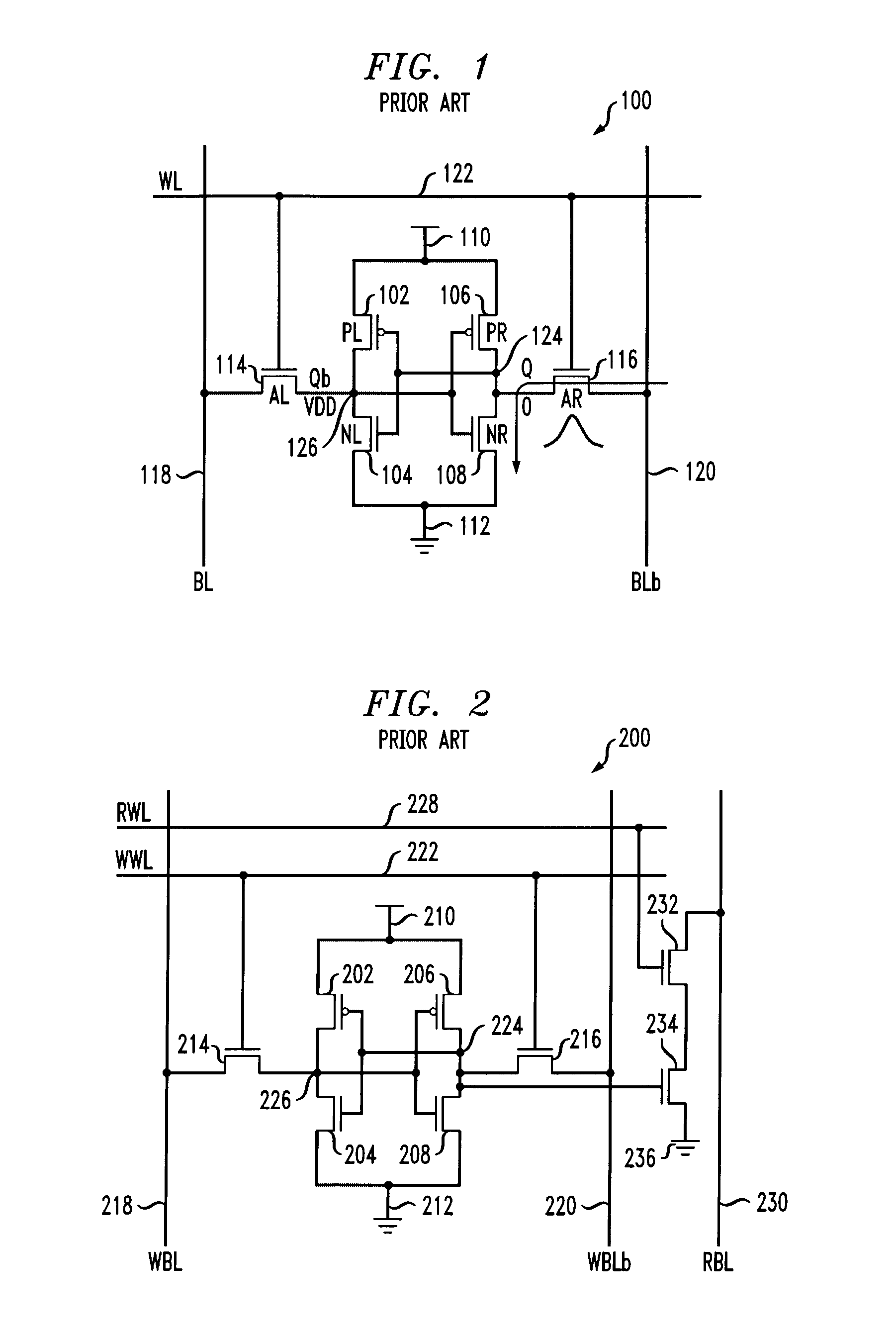
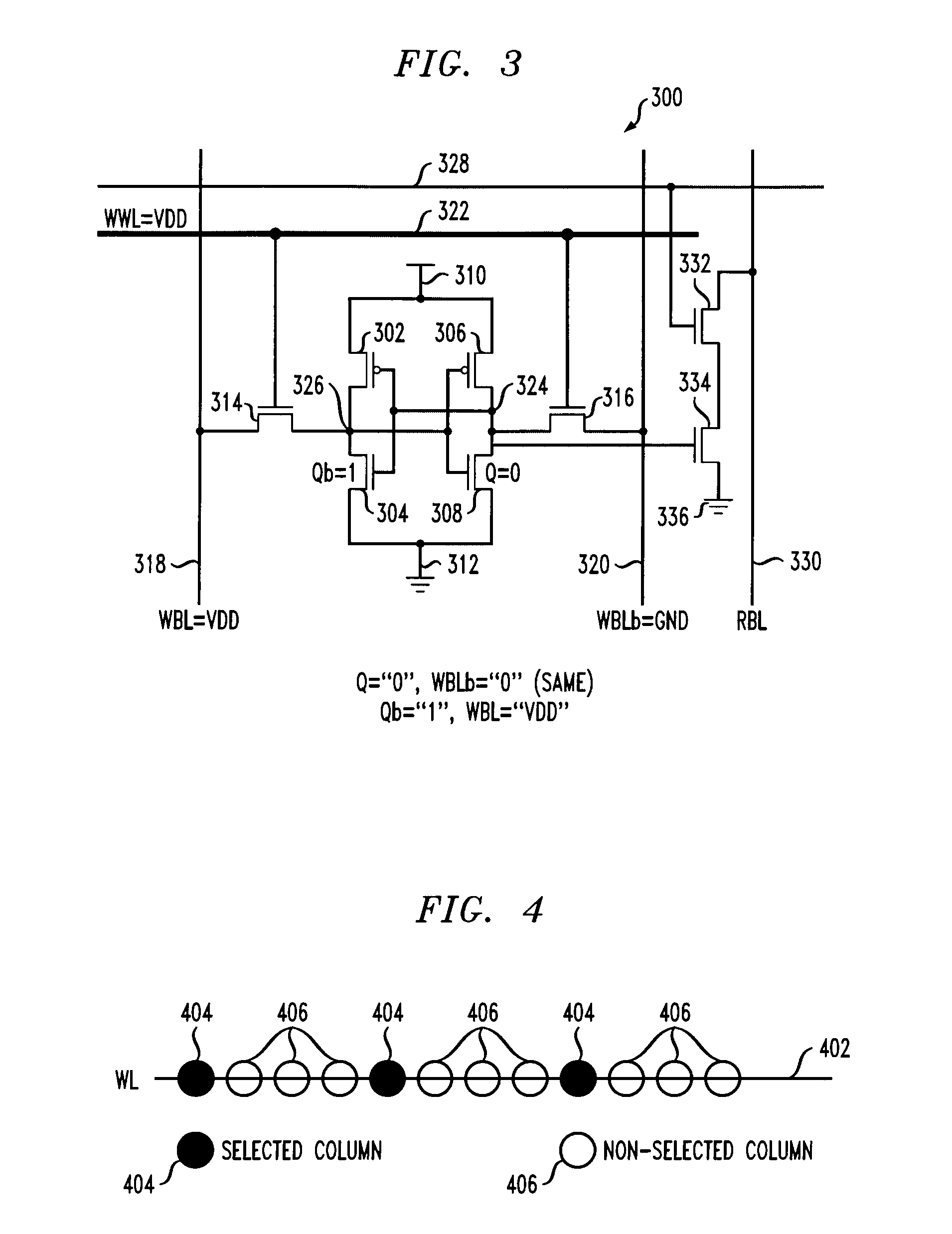
[0023]FIG. 3 shows an inventive memory cell 300. Elements in FIG. 3 similar to those in FIG. 2 have received the same reference character incremented by one hundred and will not be described again except to the extent that they differ substantially from the corresponding elements in FIG. 2. In the prior-art cell 200 of FIG. 2, during a half-select condition, when the WRITE word line 222 is raised to a high logic level (VDD), in the case when node Q stores a zero and node Qb stores a one, the true WRITE bit line 218 is at VDD, that is, the same potential as node Qb, so no current is anticipated through transistor 214. However, the complementary WRITE bit line 220 is at VDD while node Q is at a zero logic level, so noise current is anticipated through transistor 216. In the exemplary inventive cell 300, the true and complementary WRITE bit lines 318, 320 are pre-conditioned to the same voltage as the storage node voltage, to avoid a “pseudo-READ” in the half select condition. This can...


PUM


Abstract

In a memory circuit, data from all cells along a selected word line is read. Then, the read data is written back to half-selected cells and new data is written to the selected cells in the next cycle. In cases where a READ bit line (RBL) and WRITE bit line (WBL) are decoupled, RBL and WBL can be accessed simultaneously. Hence, the WRITE in the n-th cycle can be delayed to the n+1-th cycle as far as there is no data hazard such as reading data from memory before correct data are actually written to memory. As a result, there is no bandwidth loss, although the latency of the WRITE operation increases. WRITE stability issues in previous configurations with decoupled RBL and WBL are thus addressed.

Description

CROSS-REFERENCE TO RELATED APPLICATIONS[0001]This application is a continuation, under 37 CFR 1.53(b), of co-assigned U.S. patent application Ser. No. 11 / 668,545 of inventors Joshi et al., and claims the benefit thereof, said application Ser. No. 11 / 668,545 having been filed on Jan. 30, 2007, and entitled “Techniques For Improving Write Stability of Memory With Decoupled Read and Write Bit Lines.” The complete disclosure of the aforesaid application Ser. No. 11 / 668,545 is expressly incorporated herein by reference in its entirety for all purposes.FIELD OF THE INVENTION[0002]The present invention generally relates to electronic circuits and, more particularly, to electronic memory circuits.BACKGROUND OF THE INVENTION[0003]As device size shrinks down aggressively in advanced very large scale integration (VLSI) technology, increased process variation causes significant amounts of threshold voltage fluctuation. As a result, stability of static random access memory (SRAM) deteriorates du...

Claims


Application Information

Patent Timeline
Patent Type & Authority Applications(United States)
IPC IPC(8): G11C7/00
CPCG11C7/1045G11C7/12G11C11/413G11C7/22G11C11/412G11C7/18
Inventor JOSHI, RAJIV V.KIM, JAE-JOONRAO, RAHUL M.
Owner GLOBALFOUNDRIES INC
Learn More