
Phase change memory device with improved performance that minimizes cell degradation

a memory device and phase change technology, applied in the direction of information storage, static storage, digital storage, etc., can solve the problem that the stability of write data operation can be degraded in the write verification mode, and achieve the effect of reducing cell degradation, improving reliability, and increasing the stability of write data

Active Publication Date: 2011-10-20
SK HYNIX INC
View PDF5 Cites 0 Cited by
  • Summary
  • Abstract
  • Description
  • Claims
  • Application Information

AI Technical Summary

Benefits of technology

The present invention relates to a memory device with a phase change resistor that can set different reference voltage levels in a read mode and a write verifying mode to improve the stability and reliability of data storage. The device can also increase the sensing voltage margin in the read mode to enhance sensing performance. The technical effects of this invention include reducing cell degradation and improving data reliability.

Problems solved by technology

As a result, the stability of write data operation can be degraded in the write verifying mode due to cell degradation.

Method used


Image

  • Phase change memory device with improved performance that minimizes cell degradation
  • Phase change memory device with improved performance that minimizes cell degradation
  • Phase change memory device with improved performance that minimizes cell degradation

Examples


Embodiment Construction

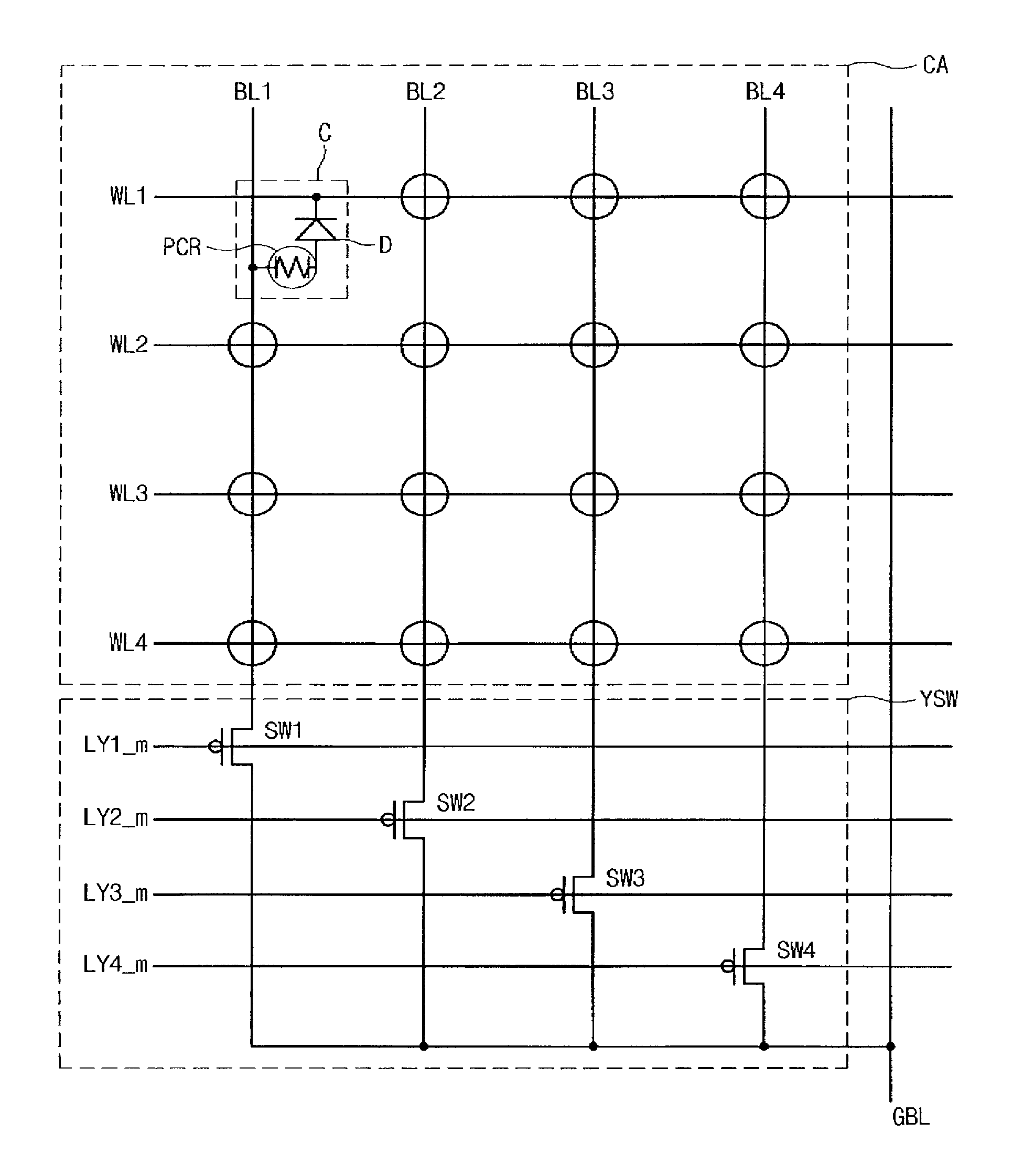
FIG. 4 is a circuit diagram illustrating a cell array and a column switching unit of a phase change memory device according to an embodiment of the present invention.

The phase change memory device of FIG. 4 comprises a cell array CA and a column switching unit YSW coupled to the cell array CA. The column switching unit YSW includes PMOS transistors SW1˜SW4. Although the column switching unit YSW is shown to include PMOS transistors in this exemplary embodiment, the present invention is understood to be not limited herein but may include any number of different electronic configures that can even include NMOS transistors.

The cell array CA includes a plurality of unit cells C positioned at intersections of bit lines BL and word lines WL. The unit cell C includes a phase change resistor PCR and a diode D. The diode D includes a PN diode element.

The phase change resistor PCR has one electrode connected to the bit line BL and the other electrode connected to a P-type region of the diode ...


PUM


Abstract

A phase change memory device having an improved performance that minimizes cell degradation is presented. The phase change memory device includes: a cell array, a sense amplifier, a write driving unit, and a reference level selecting unit. The cell array has a phase change resistor is configured to read / write data. The sense amplifier is configured to compare a reference voltage with a sensing voltage received from the cell array. The write driving unit is configured to supply a driving voltage corresponding to write data to the cell array. The reference level selecting unit is configured to select a read reference voltage in a read mode so as to output the reference voltage, and to select a reference voltage corresponding to input data in a write verifying mode so as to output the reference voltage.

Description

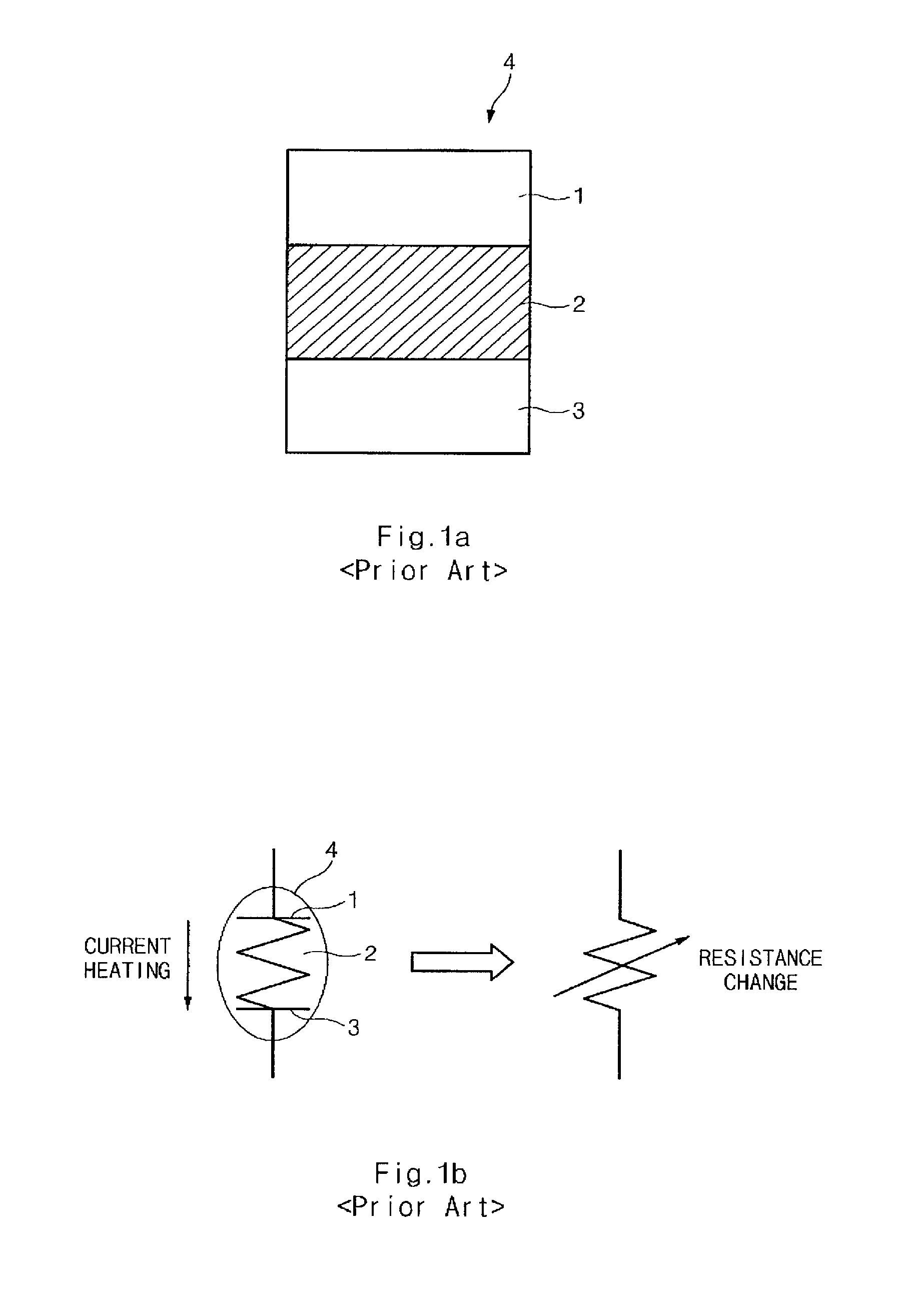
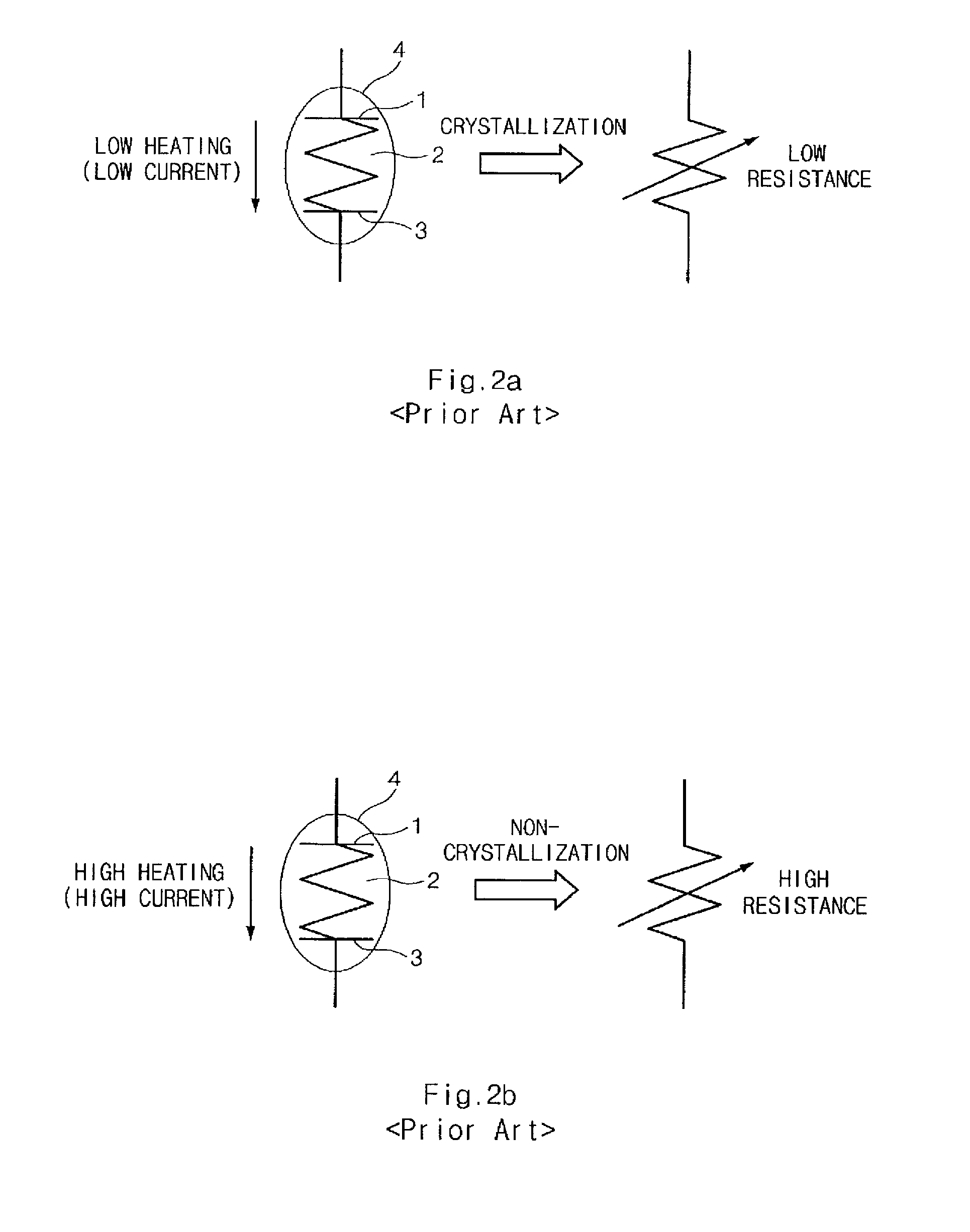
CROSS-REFERENCE TO RELATED APPLICATIONThis application is based upon and claims the benefit of priority to Korean Patent Application No. 10-2007-0104129, filed on Oct. 16, 2007, the entire contents of which are incorporated herein by reference.BACKGROUND OF THE INVENTIONThe present invention relates generally to a phase change memory device, and more particularly, to a memory device that has a phase change resistor which exhibits improved sensing performance and reliability due to resistance to memory cell degradation processes.Some well known nonvolatile memory storage devices include magnetic memory and phase change memory (PCM) devices. The PCM devices can exhibit data processing speeds similar to that of a volatile Random Access Memory (RAM) device. Further PCM devices enjoy the advantage of being able to conserve or maintain data even after the power is turned off.FIGS. 1a and 1b are diagrams illustrating a conventional phase change resistor (PCR) 4.The conventional PCR 4 compr...

Claims


Application Information

Patent Timeline
Patent Type & Authority Applications(United States)
IPC IPC(8): G11C11/21
CPCG11C11/56G11C11/5678G11C13/0004G11C13/004G11C2213/72G11C13/0069G11C2013/0054G11C2013/009G11C2211/5634G11C13/0064G11C13/02G11C5/14G11C7/06
Inventor KANG, HEE BOKHONG, SUK KYOUNG
Owner SK HYNIX INC
Learn More