Redundant temperature sensor for semiconductor processing chambers

a technology of temperature sensor and semiconductor processing chamber, which is applied in the direction of instruments, heat measurement, thermoelectric devices, etc., can solve the problems of affecting the uniformity of resulting structures, untimely deposition of reactant gas, and deterioration of the accuracy of known systems and methods for measuring and controlling temperature inside processing chambers

Active Publication Date: 2009-06-25
ASM IP HLDG BV
View PDF46 Cites 335 Cited by
  • Summary
  • Abstract
  • Description
  • Claims
  • Application Information

AI Technical Summary

Problems solved by technology

If the temperature varies across the surface of the wafer, uneven deposition of the reactant gas occurs.
Similarly, non-uniformity or instability of temperatures across a wafer during other thermal treatments can affect the uniformity of resulting structures.
However, known systems and methods for measuring and controlling temperatures inside processing chambers have been found to deteriorate in their accuracy over time or fail altogether.
These deteriorations and premature failures lead to reduced quality of depositions or unanticipated downtime for the processing chamber in order to make repairs or costly replacements.
Moreover, there is significant time and expense in returning the reactor to the operating conditions necessary to produce the desired film properties on the wafers being coated.

Method used


Image

  • Redundant temperature sensor for semiconductor processing chambers
  • Redundant temperature sensor for semiconductor processing chambers
  • Redundant temperature sensor for semiconductor processing chambers

Examples


Embodiment Construction

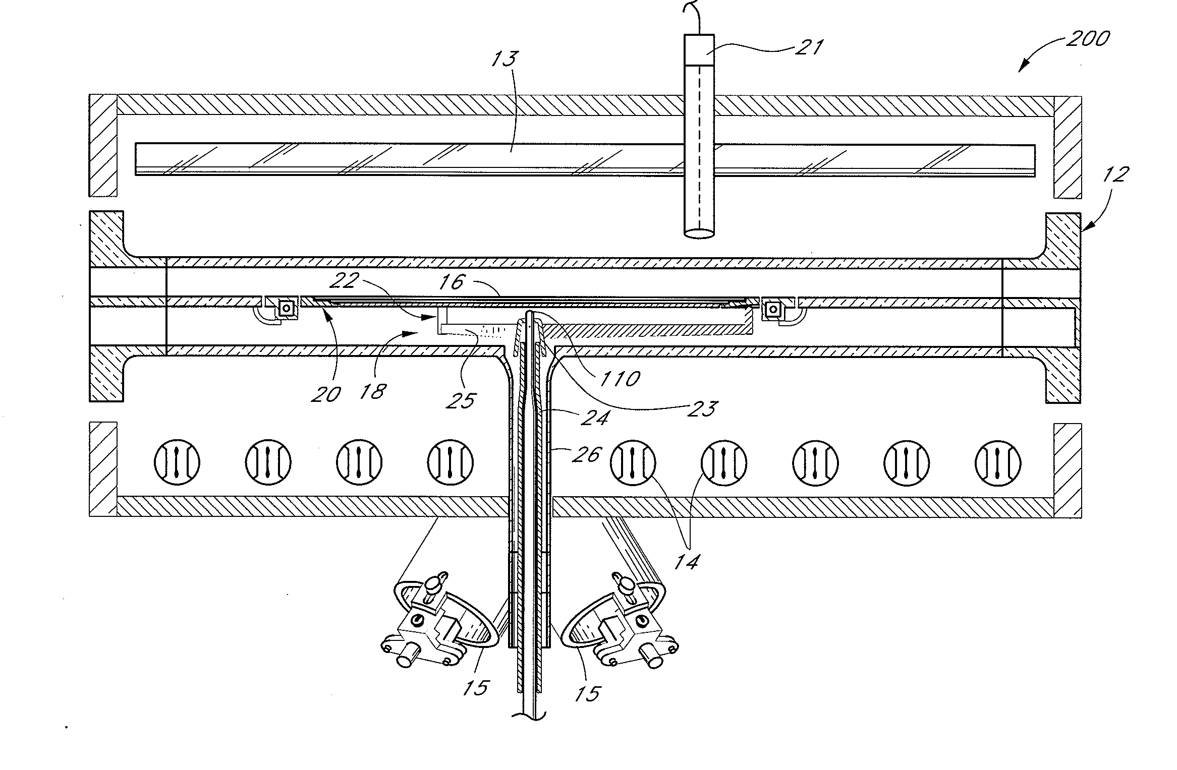
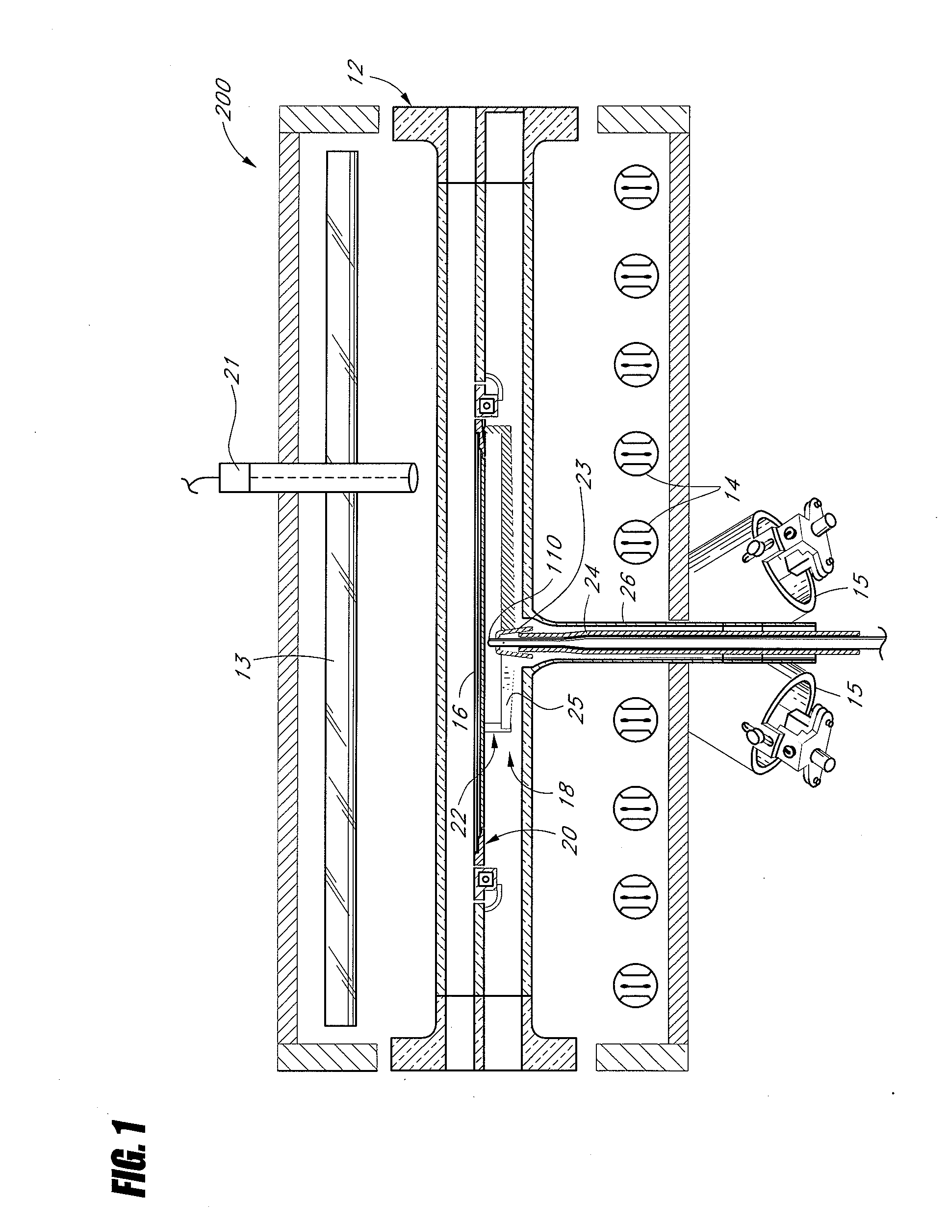
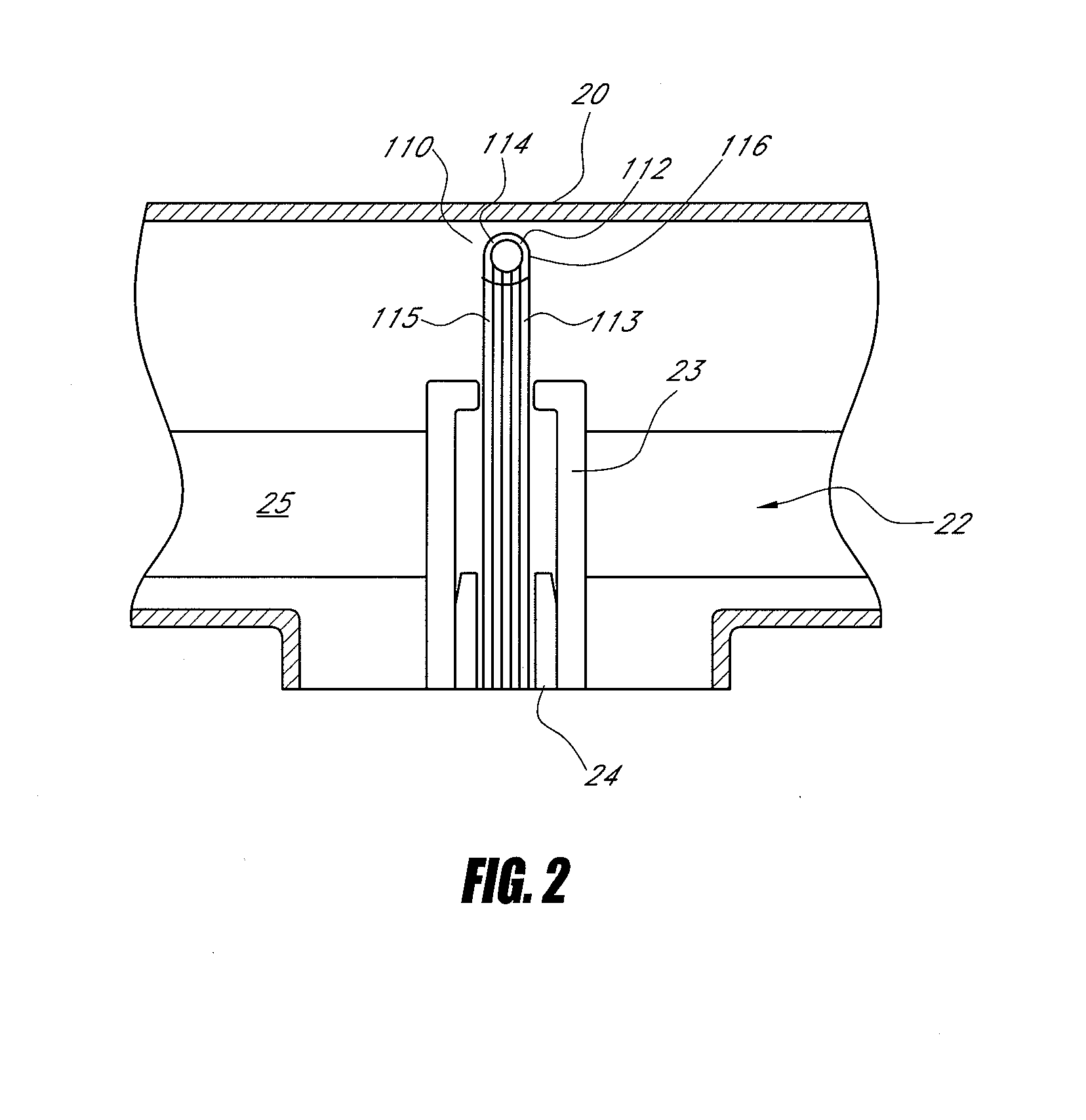
[0022]As noted above, known systems for temperature-controlled processing chambers are subject to failures that result in downtime for the reactor and significant costs for replacement components. In addition, there is significant time and expense in returning the reactor to the operating conditions necessary to produce the desired film properties on the wafer being coated. Replacing thermocouples and other components requires an intrusion into the chamber, which can result in undesirable particle generation. The methods and systems taught herein alleviate many of these problems.

[0023]While embodiments are described in the context of a cold wall CVD reactor for processing semiconductor wafers, it will be understood that the processing methods described herein will have utility in the context of reactors of other types. In particular, one of skill in the art can find applications for the methods described herein for other semiconductor processing equipment, wherein a semiconductor su...


PUM

PropertyMeasurementUnit
thicknessaaaaaaaaaa
thicknessaaaaaaaaaa
temperaturesaaaaaaaaaa

Abstract

Systems are provided for measuring temperature in a semiconductor processing chamber. Embodiments provide a multi-junction thermocouple comprising a first junction and a second junction positioned to measure temperature at substantially the same portion of a substrate. A controller may detect failures in the first junction, the second junction, a first wire pair extending from the first junction, or a second wire pair extending from the second junction. The controller desirably responds to a detected failure of the first junction or first wire pair by selecting the second junction and second wire pair. Conversely, the controller desirably responds to a detected failure of the second junction or second wire pair by selecting the first junction and first wire pair. Systems taught herein may permit accurate and substantially uninterrupted temperature measurement despite failure of a junction or wire pair in a thermocouple.

Description

BACKGROUND[0001]1. Field[0002]The present invention relates to processing substrates in semiconductor processing chambers, and more particularly to temperature sensors configured to enhance accuracy of temperature control and to reduce downtime in the reactor.[0003]2. Description of the Related Art[0004]High-temperature processing chambers are used for depositing various material layers onto semiconductor substrates. One or more substrates, such as silicon wafers, are placed on a wafer support inside the reaction chamber. Both the wafer and support are heated to a desired temperature. In a typical wafer treatment step, reactant gases are passed over the heated wafer, causing the chemical vapor deposition (CVD) of a thin layer of the reactant material on the wafer. If the deposited layer has the same crystallographic structure as the underlying silicon wafer, it is called an epitaxial layer. This is also sometimes called a monocrystalline layer because it has only one crystal structu...

Claims


Application Information

Patent Timeline
Patent Type & Authority Applications(United States)
IPC IPC(8): B05C11/00G01K7/02
CPCG01K7/04H01L21/67248G01K15/00G01K13/00
Inventor AGGARWAL, RAVINDERKLESHOCK, MARKJACOBS, LOREN
Owner ASM IP HLDG BV
Why Eureka
Try Eureka