Glitchless Clock Multiplexer Optimized for Synchronous and ASynchronous Clocks
a clock multiplexer and clock signal technology, applied in the direction of generating/distributing signals, pulse techniques, instruments, etc., can solve the problems of data integrity problems, difficult to eliminate clock line glitches, and may generate glitches on the clock lin
- Summary
- Abstract
- Description
- Claims
- Application Information
AI Technical Summary
Benefits of technology
Problems solved by technology
Method used
Image

Examples
Embodiment Construction
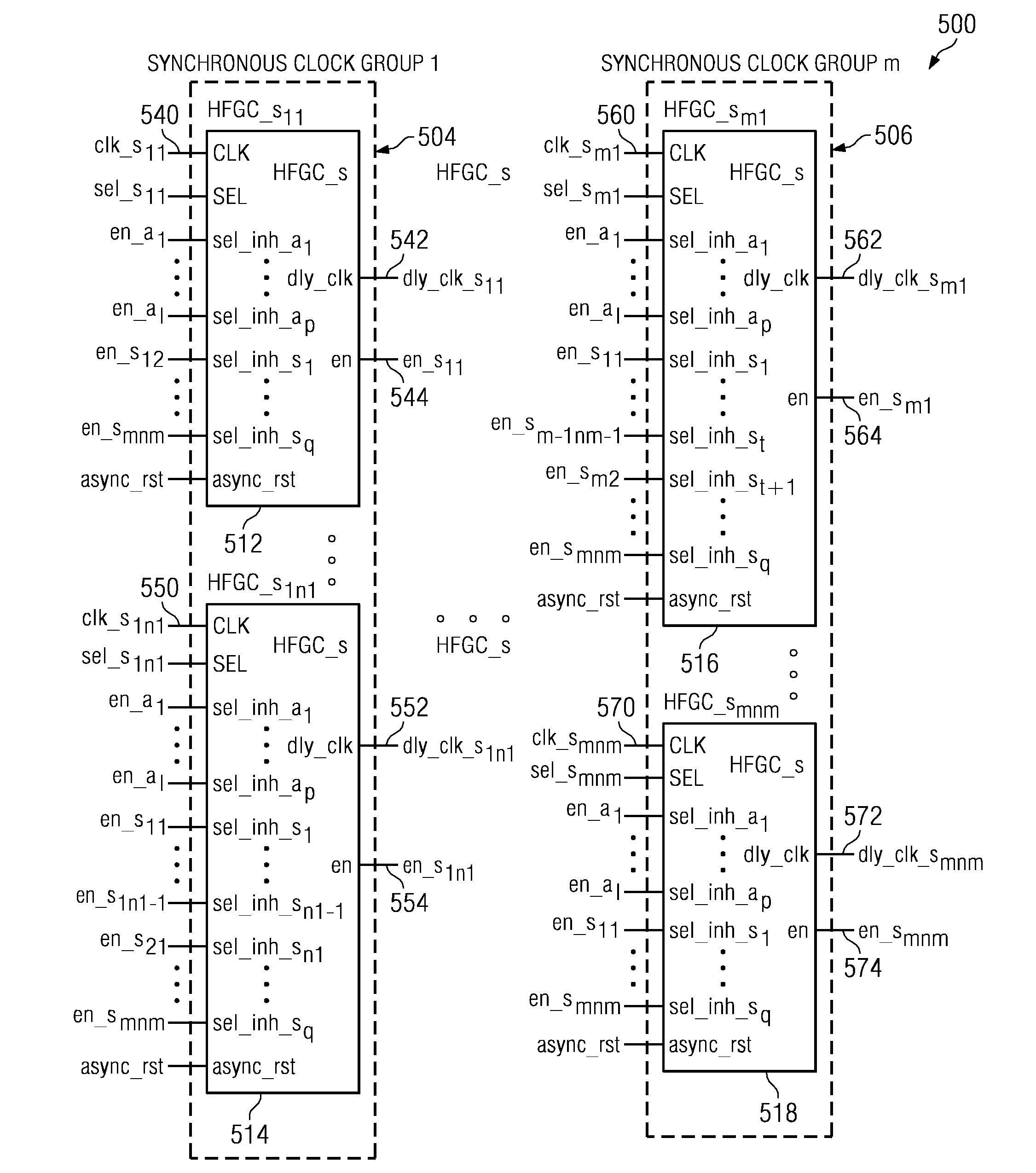
[0021]FIG. 1 is a circuit block diagram of a conventional glitchless clock multiplexer. As previously mentioned, a multiplexer is a device that selects one input clock source from several input sources and outputs the selected clock source into a single channel. Conventional glitchless clock multiplexer 100 allows for switching the source of the clock line, while avoiding a glitch on output clock line 138. The basic operation and requirement of conventional glitchless clock multiplexer 100 is to select one clock signal for output from two or more input clock sources.
[0022]In conventional glitchless clock multiplexer 100 scheme in FIG. 1, clock switching is performed with high frequency glitchless control (HFGC) blocks. In this illustrative example, conventional glitchless clock multiplexer 100 comprises n number of high frequency glitchless control blocks, including HFGC_1102, HFGC_i 104, and HFGC_n 106. The high frequency glitchless control blocks provide a delayed clock signal dly...
PUM
 Abstract
Description
Claims
Application Information
 - R&D Engineer
- R&D Manager
- IP Professional
- Industry Leading Data Capabilities
- Powerful AI technology
- Patent DNA Extraction
Browse by: Latest US Patents, China's latest patents, Technical Efficacy Thesaurus, Application Domain, Technology Topic.
© 2024 PatSnap. All rights reserved.Legal|Privacy policy|Modern Slavery Act Transparency Statement|Sitemap