Memory buffers for merging local data from memory modules

a memory buffer and local data technology, applied in the memory field, can solve the problems of slowing down the read and write access of data, bogging down the high frequency memory circuit, and adding parasitic capacitive load,

Inactive Publication Date: 2006-08-31
INTEL CORP
View PDF8 Cites 194 Cited by
  • Summary
  • Abstract
  • Description
  • Claims
  • Application Information

AI Technical Summary

Problems solved by technology

However, there are occasions when the desired data is not found in the cache memory.
If memory circuits differ, the memory read latencies and memory write latency may be inconsistent from one memory circuit to the next.
As there may be a number of memory modules plugged in, the addit

Method used


Image

  • Memory buffers for merging local data from memory modules
  • Memory buffers for merging local data from memory modules
  • Memory buffers for merging local data from memory modules

Examples


Embodiment Construction

[0019] In the following detailed description of embodiments of the invention, numerous specific details are set forth in order to provide a thorough understanding of the invention. However, it will be obvious to one skilled in the art that the embodiments of the invention may be practiced without these specific details. In other instances well known methods, procedures, components, and circuits have not been described in detail so as not to unnecessarily obscure aspects of the embodiments of the invention.

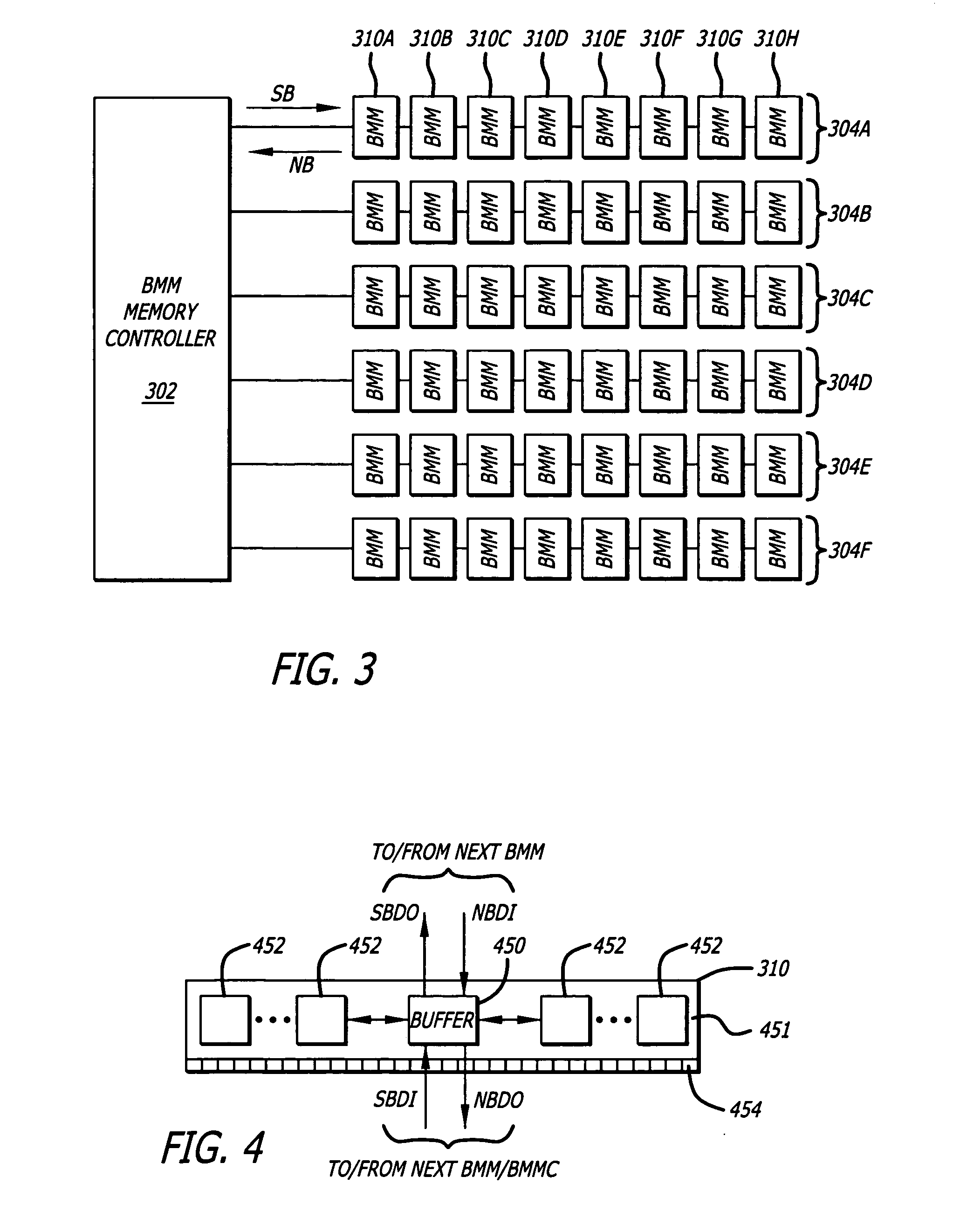
[0020] Generally the embodiments of the invention provide a data merge feature, referred to as a Northbound Data Merge (NBDM), that replaces parts of the data on a high speed link with its own data, on the fly. That is, the embodiments of the invention replace part of the incoming serial data traffic (e.g., “idle packets or frames”) over a serial data link with its local data, without having internal core logic process (e.g., serial-to-parallel conversion, assemblage into frames, ...


PUM


Abstract

An integrated circuit to serialize local data and selectively merge it with serialized feed-through data into a serial data stream output that includes a parallel-in-serial-out (PISO) shift register, a multiplexer, and a transmitter. The PISO shift register serializes parallel data on a local data bus into serialized local data. The multiplexer selectively merges serialized local data and feed-through data into a serial data stream. The transmitter drives the serial data stream onto a serial data link. In another embodiment of the invention, a method for a memory module includes receiving an input serial data stream; merging local frames of data and feed-through frames of data together into an output serial data stream in response to a merge enable signal; and transmitting the output serial data stream on a northbound data output to a next memory module or a memory controller. Other embodiments of the invention are disclosed and claimed.

Description

FIELD [0001] Embodiments of the invention relate generally to memory, and specifically to merging data from a memory buffer onto serial data channels. BACKGROUND INFORMATION [0002] In memory circuits there is typically a memory read latency that is the time period it takes for valid data to be read out of a memory circuit. A memory write latency is typically also required that is the time period to hold valid data for a memory circuit to write the data into memory. The memory read latency and the memory write latency may sometimes be buffered from a processor by a cache memory. However, there are occasions when the desired data is not found in the cache memory. In those cases, a processor may need to then read or write data with the memory circuits. Thus, the respective memory read latency or memory write latency may be experienced by the processor. If memory circuits differ, the memory read latencies and memory write latency may be inconsistent from one memory circuit to the next. ...

Claims


Application Information

Patent Timeline
IPC IPC(8): G06F3/02
CPCG06F13/1684G11C5/04G11C7/10G11C7/1051G11C7/1078G11C7/222G11C11/4093G11C2207/107G06F5/06G06F7/74G06F13/1647G06F13/1673G11C7/103G11C7/1036G06F12/00
Inventor RAJAMANI, RAMASUBRAMANIAN
Owner INTEL CORP
Why Eureka
Try Eureka