Electro-optical device, driving method of electro-optical device, and electronic apparatus

a driving method and electrooptical technology, applied in the direction of static indicating devices, non-linear optics, instruments, etc., can solve the problems of deteriorating image quality, variance in data voltage output of a plurality of amplifiers included in the drive integrated circuit, and uneven luminance in a displayed imag

Active Publication Date: 2009-07-16
138 EAST LCD ADVANCEMENTS LTD
View PDF9 Cites 24 Cited by
  • Summary
  • Abstract
  • Description
  • Claims
  • Application Information

AI Technical Summary

Benefits of technology

[0033]Advantages and effects of the invention will be apparent from the following preferred embodiments.

Problems solved by technology

However, this technique gives rise to a problem such that the data voltages output from a plurality of amplifiers included in the drive integrated circuit show variance among amplifiers when driving the electro-optical panel with the data voltages output from the drive integrated circuit.
The variance of the data voltages may be a factor of causing luminance unevenness in a displayed image.
That is, the above-mentioned technique has a technical problem in that image quality deteriorates due to variance of data voltages.
As a result, display unevenness in a line form in the data line direction occurs.
Further, in the case in which the pixel column is supplied with the data voltages from at least two different output circuits, data voltage variance between the output circuits can occur.

Method used


Image

  • Electro-optical device, driving method of electro-optical device, and electronic apparatus
  • Electro-optical device, driving method of electro-optical device, and electronic apparatus
  • Electro-optical device, driving method of electro-optical device, and electronic apparatus

Examples


first embodiment

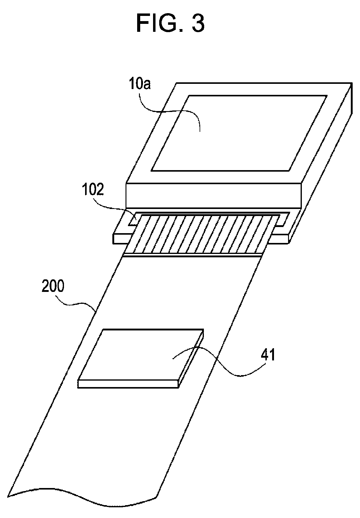
[0055]Next, a structure and an operation of an electro-optical device according to a first embodiment will be described with reference to FIGS. 3 to 7. FIG. 3 is a perspective view illustrating an entire structure of an electro-optical device according to the first embodiment. FIG. 4 is a circuit diagram illustrating a concrete structure of the electro-optical device according to the first embodiment. FIG. 5 is a circuit diagram illustrating a structure of a pixel portion. FIG. 6 is a block diagram illustrating a structure of a drive IC. FIG. 7 is a timing chart illustrating a time division operation of the electro-optical device according to the first embodiment.

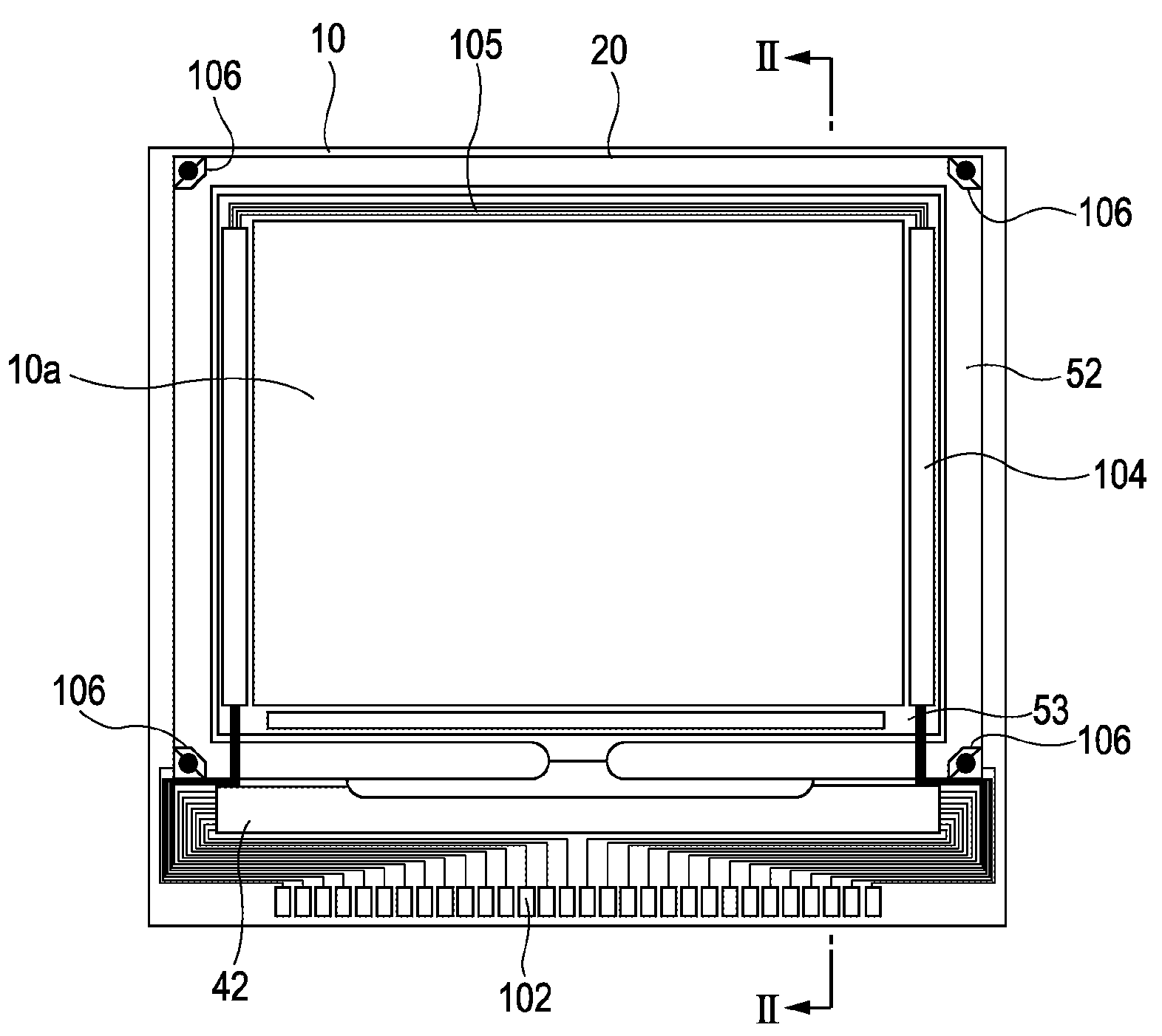
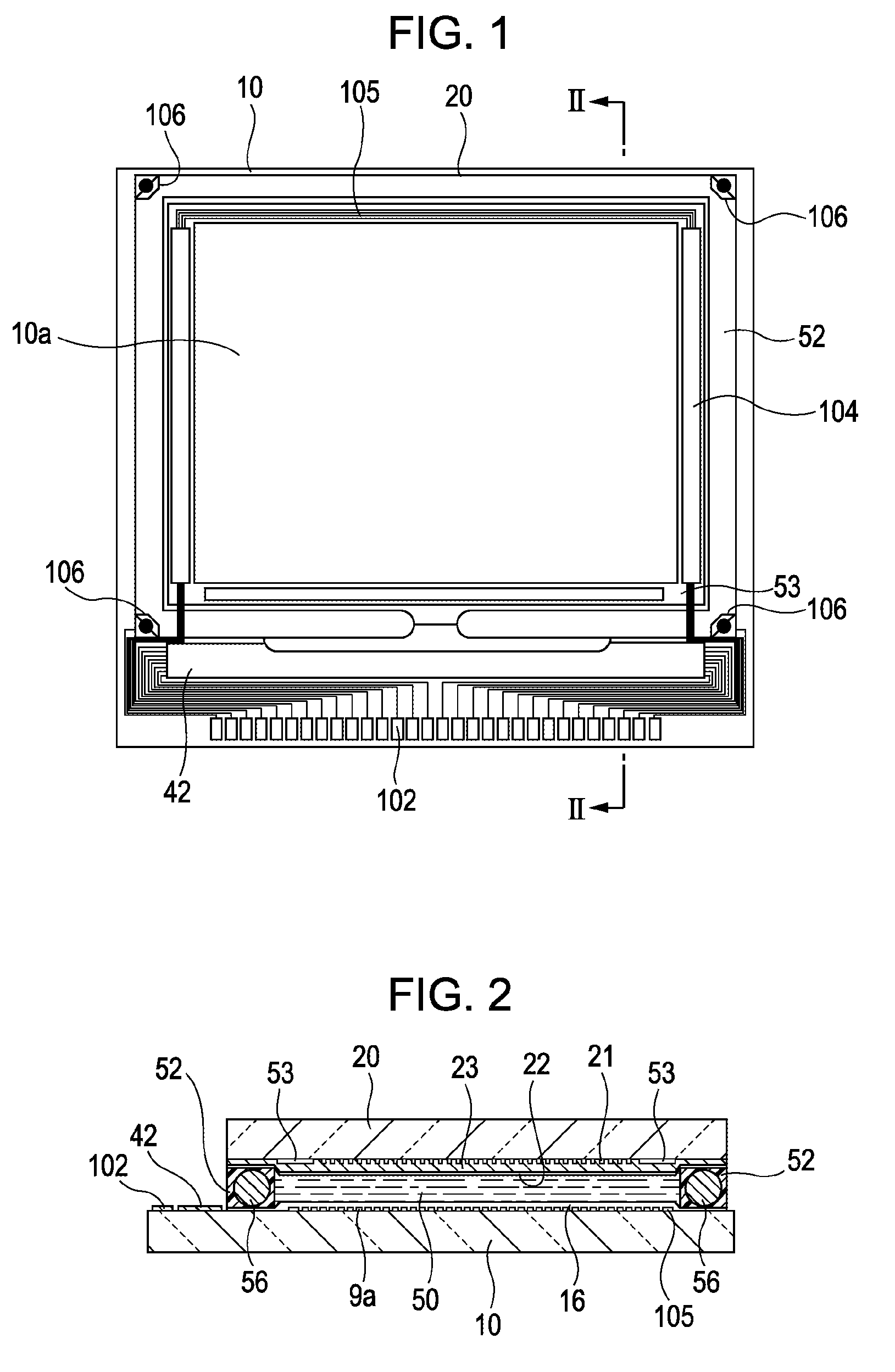
[0056]In FIG. 3, the electro-optical device according to the first embodiment includes a flexible substrate 200 which is the above-mentioned electro-optical panel and a drive IC 41 which is an example of “integrated circuit” of the invention.

[0057]The flexible substrate 200 is electrically connected to the electro-optical p...

second embodiment

[0093]Next, an electro-optical device according to the second embodiment will be described with reference to FIG. 8 and FIG. 9. FIG. 8 is a perspective view illustrating an entire structure of the electro-optical device according to the second embodiment. FIG. 9 is a circuit diagram illustrating a concrete structure of the electro-optical device according to the second embodiment. The second embodiment is different from the first embodiment in a structure of a drive IC, but other structures are the same. As for the second embodiment, points different from the first embodiment will be described. Repetitive description will be omitted. In FIG. 8 and FIG. 9, like elements between the first embodiment and the second embodiment are referenced with like references as in FIG. 3 and FIG. 4.

[0094]In FIG. 8, the electro-optical device according to the second embodiment is structured such that one electro-optical panel corresponds to two flexible substrates 200 and two drive ICs 41. In greater...


PUM


Abstract

An electro-optical device includes a pixel column, a first and second data lines, and a first and second output circuits. The pixel column including pixel portions are arranged in a first direction. The first and second data lines extend in the first direction. The first and second output circuits output data voltages to different pixel portions of the pixel column through the first and second data lines, respectively.

Description

BACKGROUND[0001]1. Technical Field[0002]The present invention relates to an electro-optical device, such as a liquid crystal display device, a driving method of an electro-optical device, and an electronic apparatus, such as a projector.[0003]2. Related Art[0004]As electro-optical devices, there is known an electro-optical device including an electro-optical panel which performs electro-optical operation, such as displaying in a pixel area, and a flexible substrate on which a drive integrated circuit which functions as at least part of a drive circuit for driving a device is formed. Such a structure of the electro-optical device enables the electro-optical panel to be realized in a small size and can make a ratio of a pixel area to the total size of the electro-optical panel increase by separating part of a control circuit from the electro-optical panel.[0005]JP-A-2005-43417 discloses a technique in which a drive integrated circuit of an electro-optical panel is provided on a flexib...

Claims


Application Information

Patent Timeline
Patent Type & Authority Applications(United States)
IPC IPC(8): G09G3/30
CPCG09G3/3611G09G3/3648G09G3/3688G09G2300/0426G09G2310/0205G09G3/34G09G2310/0251G09G2310/027G09G2310/0281G09G2310/0297G09G2320/0233G09G2310/0218G02F1/133G09G3/20G09G3/36
Inventor ITO, AKIHIKO
Owner 138 EAST LCD ADVANCEMENTS LTD
Why Eureka
Try Eureka