Full Color CMOS Imager Filter

a cmos imager and filter technology, applied in the field of integrated circuit (ic) fabrication, can solve the problems of limiting the fabrication of cmos imagers using adding to the cost of the color filter, and limiting the use of cmos imagers with a smaller pixel size, so as to improve the color separation and broaden the spectrum of photorespons

Active Publication Date: 2009-08-13
SHARP KK
View PDF6 Cites 56 Cited by
  • Summary
  • Abstract
  • Description
  • Claims
  • Application Information

AI Technical Summary

Benefits of technology

[0017]Presented is a color filter to improve the color separation in a CMOS imager using two stand-alone pixels for three color detection. As an example, a green-absorbing filter (also known as a magenta filter) may be added to the stacked photodiode pixel to suppress green light from entering the photodiodes, so the blue and red photodiodes have spectra with depressed green color absorption. A green-transmitting filter may optionally be added to the single photodiode pixel. If no filter is used over the “green” diode, the spectrum of the photoresponse is broad. However, by subtracting the sum of the red and blue diode signals from that of the broad “green” diode, a narrower green color response may be recovered. This subtraction process may be implemented as part of the color conversion algorithms.

Problems solved by technology

Misalignment of the color filter results in color artifacts, and the color filter adds to the cost of the imager.
Therefore, a wider isolation region is required, which in turn, limits the imager pixel size.
These processes limit the fabrication of CMOS imagers using a smaller pixel size.
However, the integrating of two or three epitaxial layers is very complex.
In addition, it is well known the interface between epi layer is a relatively large leakage current source, making a low dark current sensor difficult to fabricate.
However, without precautions, such a structure may result in significant color overlap between the diodes.

Method used


Image

  • Full Color CMOS Imager Filter
  • Full Color CMOS Imager Filter
  • Full Color CMOS Imager Filter

Examples


Embodiment Construction

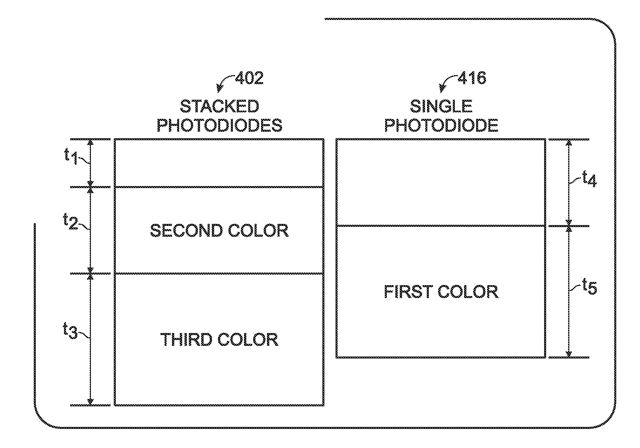
[0034]FIG. 4 is a partial cross-sectional view of a dual-pixel full color CMOS imager. The imager 400 comprises a two-photodiode stack 402 including an n doped substrate 404, a bottom photodiode 406, and a top photodiode 408. The bottom photodiode 406 includes a bottom p doped layer 410 overlying the substrate 404 and a bottom n doped layer cathode 412 overlying the bottom p doped layer 410. The top photodiode 408 has a top p doped layer 413 overlying the bottom n doped layer 412 and a top n doped layer cathode 414 overlying the top p doped layer 413. A single photodiode 416 includes the n doped substrate 404, a p doped layer 418 overlying the substrate 404, and an n doped layer cathode 420 overlying the p doped layer 418.

[0035]An n doped region, as defined herein, is associated with dopant concentrations in the range of about 1×10¹⁵ to 5×1017 cm−3, the n+ doped floating diffusion areas have dopant concentrations in the range of about 1×10¹⁹ to 1×1021 cm−3. For the p doped regions, ...


PUM


Abstract

A full color complementary metal oxide semiconductor (CMOS) imaging circuit is provided. The imaging circuit comprises an array of photodiodes including a plurality of pixel groups. Each pixel group supplies 3 electrical color signals, corresponding to 3 detectable colors. The circuit also includes a color filter array overlying the photodiode array employing less than 3 separate filter colors. Each pixel group may be enabled as a dual-pixel including a single photodiode (PD) to supply a first color signal and stacked PDs to supply a second and third color signal. In one aspect, the color filter array employs 1 filter color per pixel group. In another aspect, the color filter array employees 2 filter colors per pixel group. In either aspect, the color filter array forms a checkerboard pattern of color filter pixels. For example, a magenta color filter may overlie the stacked PDs of each dual-pixel, to name one variation.

Description

RELATED APPLICATIONS[0001]This application is a continuation-in-part of a pending patent application entitled, DUAL-PIXEL FULL COLOR CMOS IMAGER, invented by Lee et al., Ser. No. 12 / 025,618, filed Feb. 4, 2008, attorney docket no. SLA2260, which is incorporated herein by reference.BACKGROUND OF THE INVENTION[0002]1. Field of the Invention[0003]This invention generally relates to integrated circuit (IC) fabrication and, more particularly, a dual-pixel full color imager filter.[0004]2. Description of the Related Art[0005]FIG. 1 depicts a complementary metal oxide semiconductor (CMOS) imager with a “buried” or “pinned” photodiode (prior art). Conventionally, the image cell circuit includes four transistors and one photodiode. The pixel operation is divided into three main stages: reset, exposure, and reading.[0006](1) The reset stage: by turning on the reset and transfer (Tx) transistors, the photodiode capacitance is charged to a reset voltage. As for the case of the p+np buried photo...

Claims


Application Information

Patent Timeline
Patent Type & Authority Applications(United States)
IPC IPC(8): H01L31/02
CPCH01L27/14621H01L27/14641H01L27/14647H01L27/14645
Inventor TWEET, DOUGLAS J.LEE, JONG-JAN
Owner SHARP KK
Why Eureka
Try Eureka