Array substrate and manufacturing method thereof, display panel and display device

A technology for array substrates and display panels, applied in semiconductor/solid-state device manufacturing, diodes, semiconductor devices, etc., can solve the problems of low reliability of OLED display panels, improve color separation, improve surface flatness, and improve product reliability degree of effect

Active Publication Date: 2021-04-09
BOE TECH GRP CO LTD
View PDF8 Cites 0 Cited by
  • Summary
  • Abstract
  • Description
  • Claims
  • Application Information

AI Technical Summary

Problems solved by technology

[0005] Embodiments of the present invention provide an array substrate and its manufacturing method, a display panel, and a display device, which can solve the problem of low reliability of OLED display panels in the related art

Method used


Image

  • Array substrate and manufacturing method thereof, display panel and display device
  • Array substrate and manufacturing method thereof, display panel and display device
  • Array substrate and manufacturing method thereof, display panel and display device

Examples


Embodiment Construction

[0052] In order to make the objectives, technical solutions and advantages of the present invention clearer, the embodiments of the present invention will be further described in detail below with reference to the accompanying drawings.

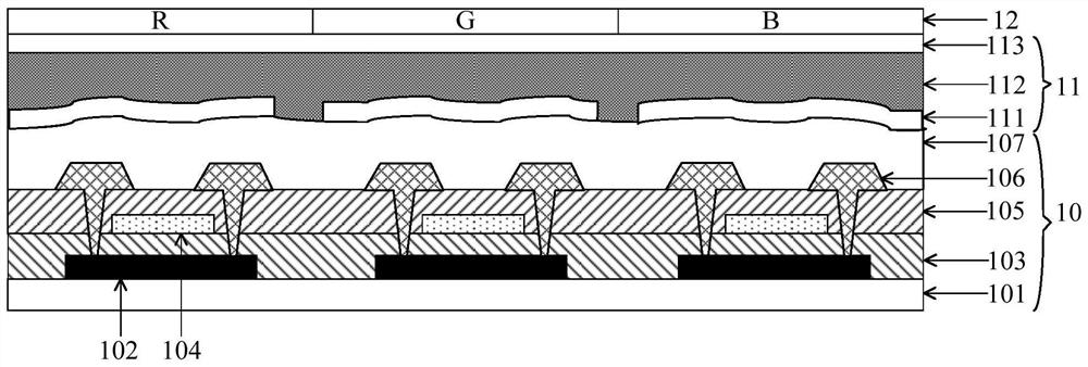
[0053] figure 1It is a schematic structural diagram of an OLED display panel provided in the related art, such as figure 1 As shown, the OLED display panel includes an array substrate 10 , a light-emitting device 11 located on the array substrate 10 , and a filter 12 located on the light-emitting side of the light-emitting device 11 . see figure 1 , the array substrate 10 includes a base substrate 101, and an active layer 102, a passivation layer 103, a gate pattern 104, an interlayer insulating layer 105, a source-drain pattern 106 and a flat layer 107 stacked on the base substrate 101 ; The light-emitting device 11 includes a first electrode 111, a light-emitting layer 112 and a second electrode 113; the filter 12 has a red filter area R,...


PUM

PropertyMeasurementUnit
thicknessaaaaaaaaaa

Abstract

The invention discloses an array substrate and a manufacturing method thereof, a display panel and a display device, belonging to the technical field of display. The array substrate has a display area and a non-display area around the display area, the array substrate includes a base substrate, and gate patterns, interlayer insulating layers, flat patterns and source / drain patterns sequentially arranged on the base substrate wherein, the flat pattern is complementary to the source and drain patterns in the display area, and the flat pattern has a first slot for accommodating the source and drain patterns in the display area. The invention improves the flatness of the array substrate by arranging in the display area a flat pattern complementary to the shape of the source and drain patterns in the display area, thereby improving the color separation phenomenon.

Description

technical field [0001] The present invention relates to the field of display technology, and in particular, to an array substrate and a manufacturing method thereof, a display panel and a display device. Background technique [0002] Organic Light-Emitting Diode (OLED), as a current-type light-emitting device, has the characteristics of low power consumption, self-luminescence, high color saturation, fast response, wide viewing angle and flexibility. It is increasingly used in the field of high-performance displays. The current OLED display panel generally adopts circular polarizer (English: Circular Polarizer) to reduce the external reflected light, that is, the circular polarizer is attached to the light-emitting surface of the OLED display panel, and the circular polarizer can reduce the environment entering the OLED display panel. The amount of light emitted from the light-emitting surface after being reflected by the internal structure of the OLED display panel. [00...

Claims


Application Information

Patent Timeline
Patent Type & Authority Patents(China)
IPC IPC(8): H01L27/32H01L51/56
CPCH01L27/1248H10K59/353H10K59/124H10K59/1213H10K71/40H10K71/20H01L29/78618H10K59/121H10K59/38H10K71/00H10K59/1201
Inventor 田宏伟牛亚男李栋王纯阳刘明刘政
Owner BOE TECH GRP CO LTD
Why Eureka
Try Eureka