Contactless communication device

a communication device and contactless technology, applied in the field of contactless integrated circuits, can solve the problems of overall dimensions, bandwidth and data collision problems, and each of them must have a bulky antenna, and achieve the effect of maximizing the confinement of magnetic fields

Active Publication Date: 2009-09-10
COMMISSARIAT A LENERGIE ATOMIQUE ET AUX ENERGIES ALTERNATIVES
View PDF6 Cites 20 Cited by
  • Summary
  • Abstract
  • Description
  • Claims
  • Application Information

AI Technical Summary

Benefits of technology

[0028]In other words, using strong coupling between the chip antennas and the bus antenna and choosing surface areas which are substantially equal maximizes confinement of the magnetic fields which are us

Problems solved by technology

Integrating several chips on a single substrate does, however, pose the problem of overall dimensions which is linked to communication distances.
Consequently, simply placing several contactless chips side-by-side on a single card means that each of them must have a bulky antenna in order to achieve an adequate communication range.
In addition, in many applications, some chips are not designed to communicate with a

Method used


Image

  • Contactless communication device
  • Contactless communication device
  • Contactless communication device

Examples


Embodiment Construction

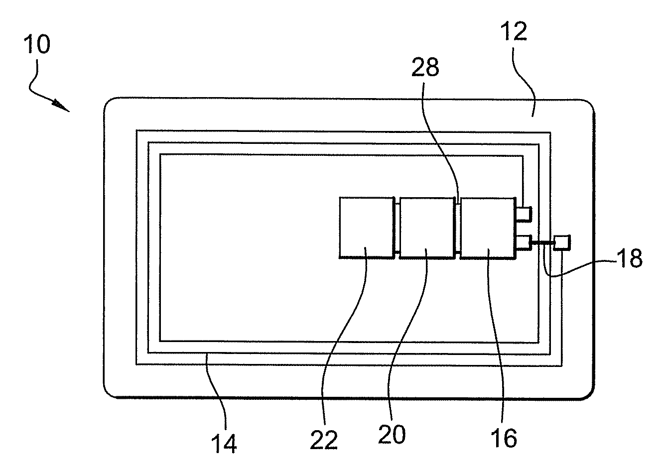
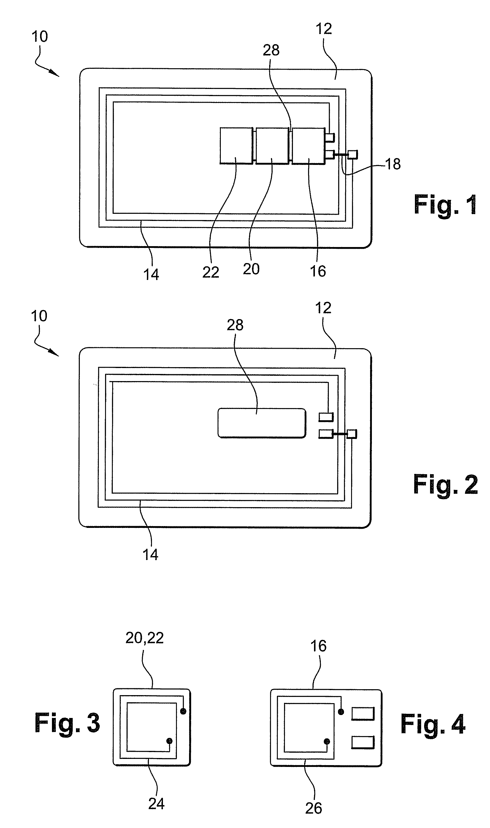
[0043]A multi-chip contactless card, which complies with Standard ISO 14443 for example, is shown in FIGS. 1 to 3 and referred to in its entirety as 10. Contactless card 10 comprises a rectangular substrate 12, which is made of plastic for example, on or in which there is a large antenna 14 which forms several inductive loops around the periphery of card 10. Antenna 14 is referred to subsequently as a “card” antenna.

[0044]Card 10 also comprises a chip 16 which is referred to as a “master” chip and is electrically connected to card antenna 14, realized for example by means of connections 18 realized using a “flip-chip” technique. Master chip 16 allows card 10 to communicate with its external environment by means of card antenna 14, e.g. contactless communication with a reader (not shown).

[0045]Several contactless chips 20, 22 are also provided on card 10, these chips are referred to as “slaves” because they are not electrically connected to card antenna 14.

[0046]Each of chips 16, 20,...


PUM


Abstract

The invention relates to a device comprising a first inductive antenna and a plurality of chips, each comprising an integrated circuit and a second inductive antenna used to power and communicate with said integrated circuit. According to the invention, one chip amongst the plurality of chips is capable of being connected to first inductive antenna. In addition, the device comprises a third inductive antenna which is inductively coupled to each of the second antennas of the plurality of chips.

Description

FIELD OF THE INVENTION[0001]The present invention relates to the field of contactless integrated circuits such as contactless smart cards of the type described in Standard ISO 14443 which are capable of receiving and transmitting data by inductive coupling through an antenna.DESCRIPTION OF THE PRIOR ART[0002]The increasing need to integrate several contactless chips on a single substrate is making itself felt in particular because of growing demand for memory and security.[0003]Integrating several chips on a single substrate does, however, pose the problem of overall dimensions which is linked to communication distances. In fact, contactless cards transmit their data with the aid of a magnetic field, the power of which depends on the size of their on-chip inductive antenna. Consequently, simply placing several contactless chips side-by-side on a single card means that each of them must have a bulky antenna in order to achieve an adequate communication range.[0004]To overcome this pr...

Claims


Application Information

Patent Timeline
IPC IPC(8): G06K19/067
CPCG06K19/072G06K19/07749G06K19/0723
Inventor SAVRY, OLIVIER
Owner COMMISSARIAT A LENERGIE ATOMIQUE ET AUX ENERGIES ALTERNATIVES
Why Eureka
Try Eureka