Semiconductor laser device

a laser device and semiconductor technology, applied in semiconductor lasers, laser details, optical resonator shape and construction, etc., can solve the problems of difficult design of cavity structures and difficult implementation of long-wavelength laser devices, and achieve the effect of expanding the polarization field

Inactive Publication Date: 2009-10-08
ROHM CO LTD
View PDF2 Cites 61 Cited by
  • Summary
  • Abstract
  • Description
  • Claims
  • Application Information

AI Technical Summary

Benefits of technology

[0011]If the In composition is increased for wavelength elongation, the polarization field is enlarged and hence a blueshift resulting from the shielding of the polarization field more remarkably appears.

Problems solved by technology

Due to such blueshifts, it is difficult to design a cavity structure, particularly reflector structures on the cavity end faces, and a long-wavelength laser device is consequently hard to implement.

Method used


Image

  • Semiconductor laser device
  • Semiconductor laser device
  • Semiconductor laser device

Examples


Embodiment Construction

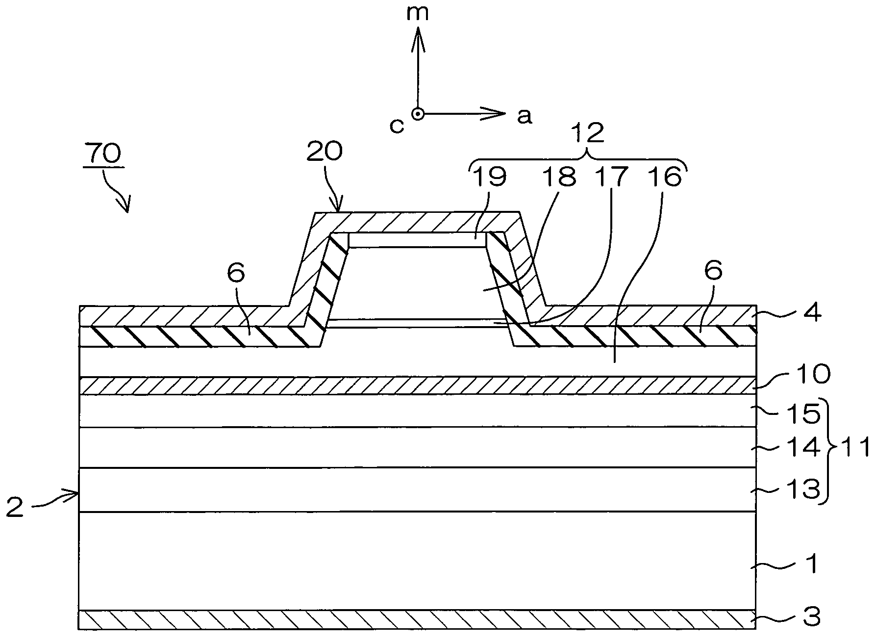
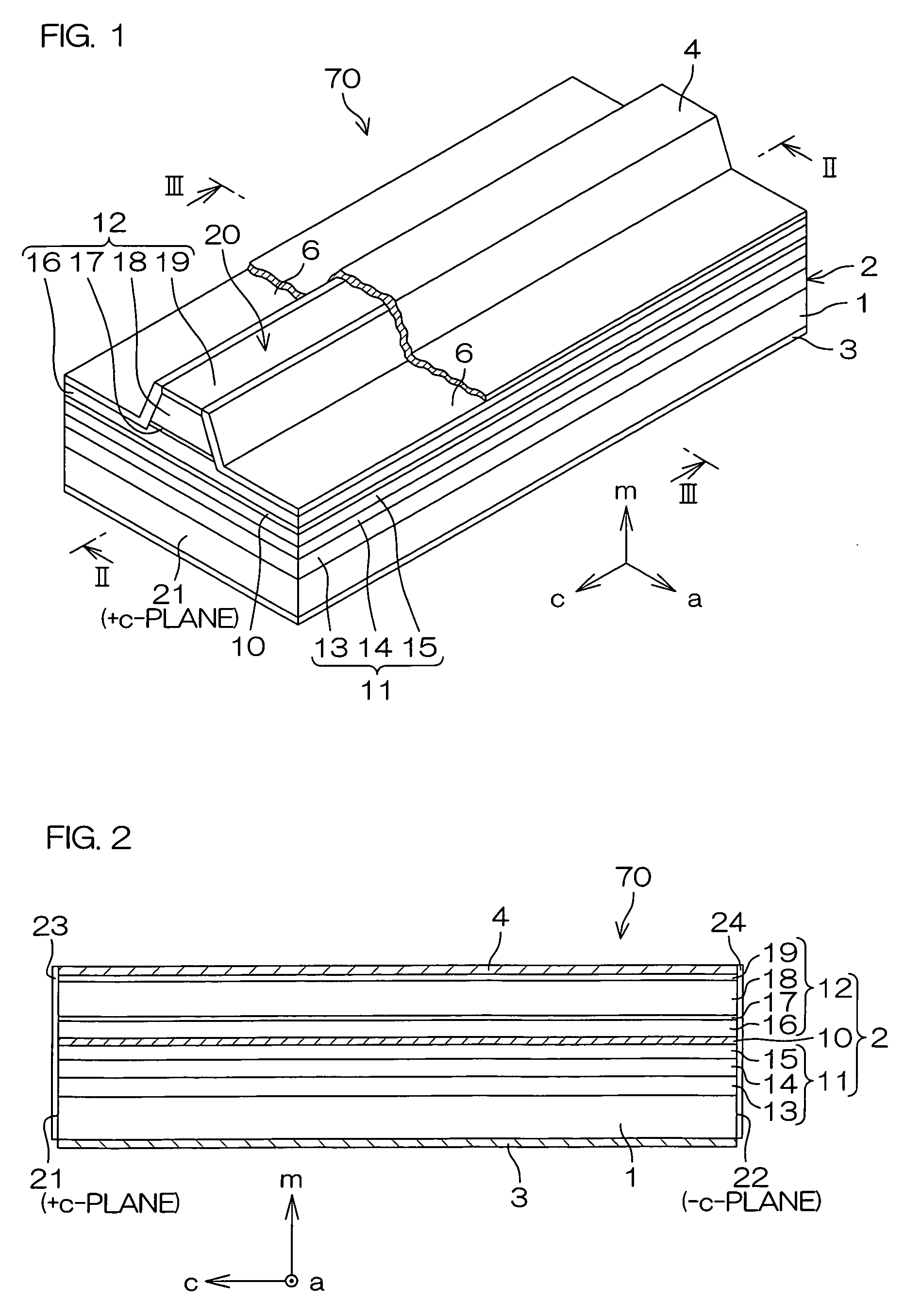
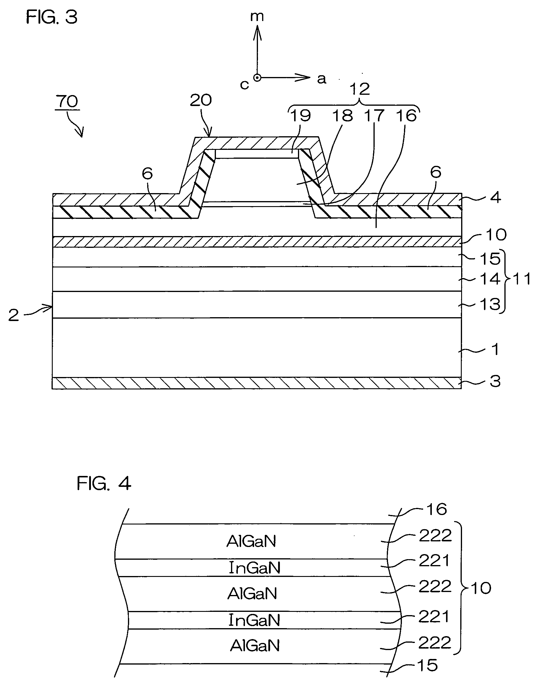
[0033]A semiconductor laser device according to an embodiment of the present invention is made of a group III nitride semiconductor having a major growth surface defined by a nonpolar plane or a semipolar plane. The semiconductor laser device includes a cavity including an active layer containing In and distributed Bragg reflectors coating both cavity end faces of the cavity respectively. In each of the distributed Bragg reflectors, a central wavelength λc of a reflectance spectrum satisfies the relation λSP−10 nm≦λc≦λSP+10 nm with respect to an emission peak wavelength λSP of spontaneous emission in the active layer.

[0034]According to the structure, the semiconductor laser device is constituted of the group III nitride semiconductor having the major growth surface defined by a nonpolar plane or a semipolar plane. Spontaneous piezoelectric polarization in the active layer disappears when the major growth surface is defined by a nonpolar plane, while the spontaneous piezoelectric pol...


PUM


Abstract

A semiconductor laser device is made of a group III nitride semiconductor having a major growth surface defined by a nonpolar plane or a semipolar plane. The semiconductor laser device includes a cavity having an active layer containing In and distributed Bragg reflectors coating both cavity end faces of the cavity respectively. In each of the distributed Bragg reflectors, a central wavelength λc of a reflectance spectrum satisfies the relation λSP−10 nm≦λc≦λSP+10 nm with respect to an emission peak wavelength λSP of spontaneous emission in the active layer.

Description

BACKGROUND OF THE INVENTION[0001]1. Field of the Invention[0002]The present invention relates to a semiconductor laser device employing group III nitride semiconductors.[0003]2. Description of Related Art[0004]Group III nitride semiconductors are group III-V semiconductors employing nitrogen as a group V element, and typical examples thereof include aluminum nitride (AlN), gallium nitride (GaN) and indium nitride (InN), which can be generally expressed as AlXInYGa1-X-YN (0≦X≦1, 0≦Y≦1 and 0≦X+Y≦1).[0005]A blue or green wavelength laser source is increasingly used in the fields of an full color display, high-density recording in an optical disk represented by a DVD, image processing, medical equipment, measuring equipment and the like. Such a laser source is comprised of a laser diode employing GaN semiconductors, for example.[0006]A GaN semiconductor laser diode is manufactured by growing group III nitride semiconductors on a gallium nitride (GaN) substrate having a major surface def...

Claims


Application Information

Patent Timeline
Patent Type & Authority Applications(United States)
IPC IPC(8): H01S5/00
CPCB82Y20/00H01S5/028H01S5/34333H01S5/2004H01S5/3211H01S5/0288
Inventor KUBOTA, MASASHIOKAMOTO, KUNIYOSHITANAKA, TAKETOSHI
Owner ROHM CO LTD
Why Eureka
Try Eureka