Measurement apparatus, exposure apparatus, and device manufacturing method
a technology of exposure apparatus and measurement apparatus, which is applied in the direction of measurement devices, instruments, printing, etc., can solve the problems of measurement value being known to have an error, the detection error of the surface position of the substrate attributed to the performance of the optical system which detects the surface position is becoming non-negligible, and the depth of focus is extremely low.
- Summary
- Abstract
- Description
- Claims
- Application Information
AI Technical Summary
Benefits of technology
Problems solved by technology
Method used
Image

Examples
first embodiment
[0032]FIG. 8 is a view showing the schematic arrangement of an exposure apparatus according to a preferred embodiment of the present invention. An exposure apparatus EX according to a preferred embodiment of the present invention includes an illumination unit 800, an original stage RS which holds an original (reticle) 31, a projection optical system 32, a substrate stage WS which holds a substrate (e.g., a wafer) 6, and a control unit 1100 as a basic configuration. A reference plate 39 is arranged on the substrate stage WS. The pattern of the original 31 illuminated by the illumination unit 800 is projected onto a substrate 6 by the projection optical system 32 to expose the substrate 6. The substrate 6 is coated with a photoresist, on which a latent image pattern is formed by exposure.
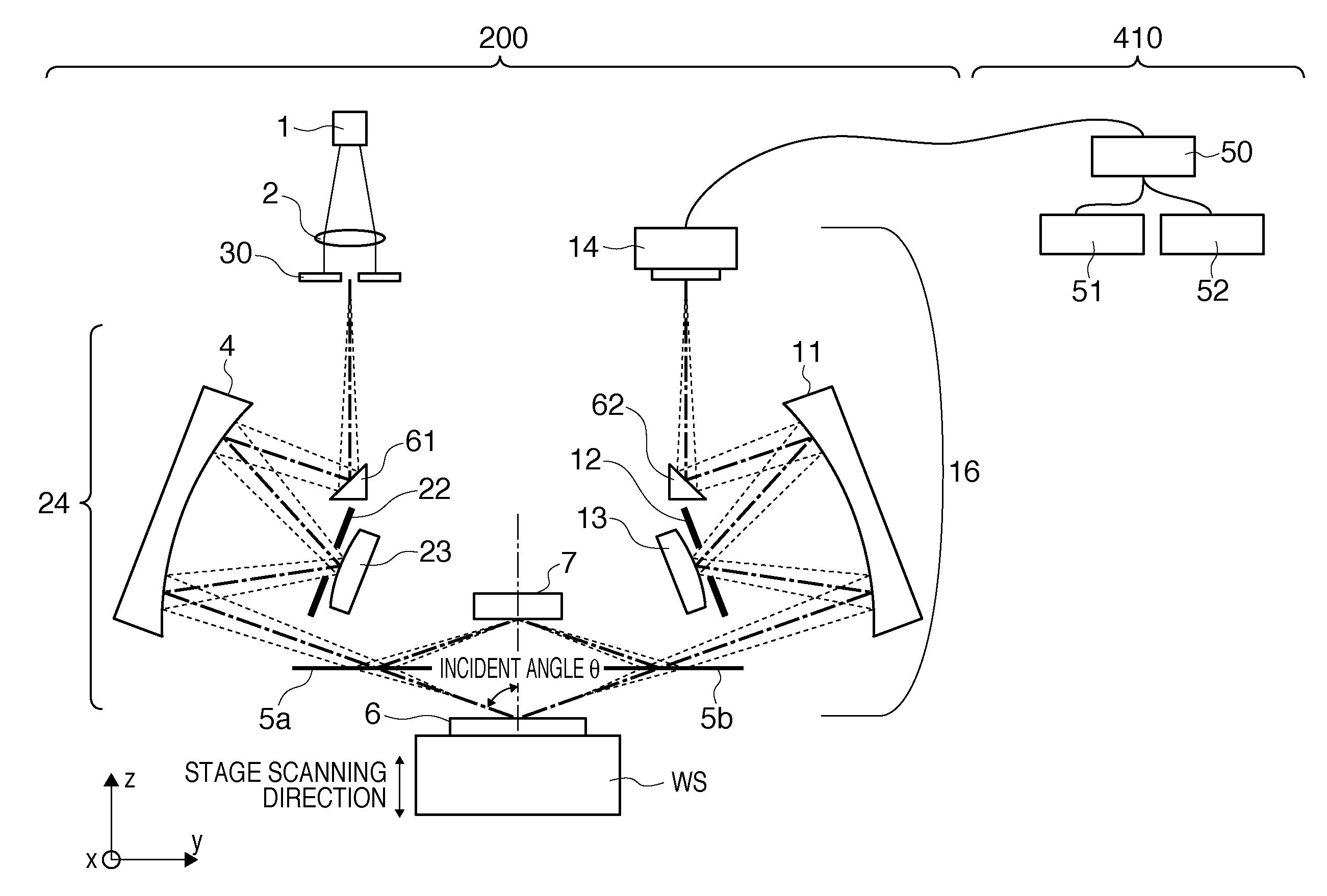
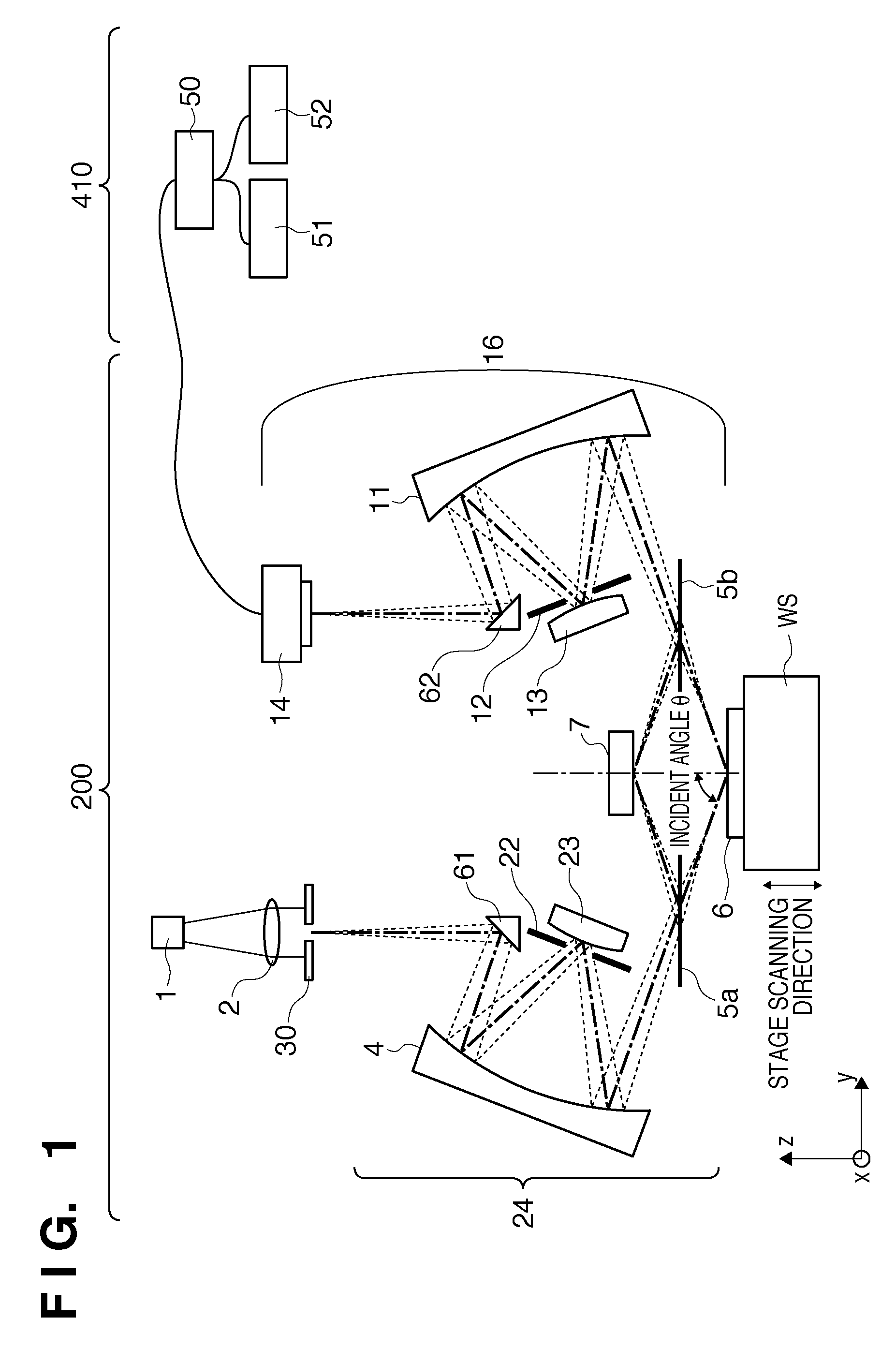
[0033]The exposure apparatus EX also includes a surface position measurement interferometer (first measurement device) 200 and focus control sensor (second measurement device) 33 as measurement device...
second embodiment
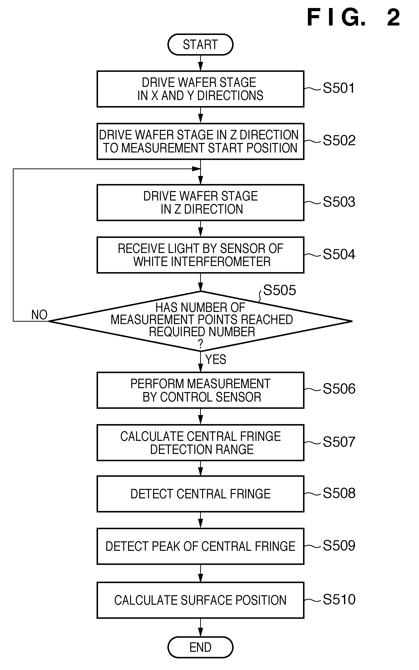
[0102]An exemplary procedure for calculating the central fringe detection range by the focus control sensor 33 after acquiring a white light interference signal has been explained in the first embodiment. An exemplary procedure for determining the central fringe detection range using a focus control sensor 33 in advance, and acquiring a white light interference signal in this range will be explained in the second embodiment.
[0103]FIG. 3 is a flowchart showing a sequence according to the second embodiment of the present invention. This sequence can be controlled by a CPU 50 of an arithmetic processing unit 410.
[0104]First, in step S601, a substrate stage WS is driven in the X and Y directions to be able to measure the measurement target region on a substrate 6. In step S602, the substrate stage WS is driven in the Z direction to be able to measure the surface position of the substrate 6 by the focus control sensor 33.
[0105]In step S603, the surface position of the substrate 6 in its ...
PUM
 Abstract
Description
Claims
Application Information
 - R&D Engineer
- R&D Manager
- IP Professional
- Industry Leading Data Capabilities
- Powerful AI technology
- Patent DNA Extraction
Browse by: Latest US Patents, China's latest patents, Technical Efficacy Thesaurus, Application Domain, Technology Topic.
© 2024 PatSnap. All rights reserved.Legal|Privacy policy|Modern Slavery Act Transparency Statement|Sitemap