Three dimensional stacked nonvolatile semiconductor memory

a nonvolatile, semiconductor technology, applied in semiconductor devices, semiconductor/solid-state device details, electrical devices, etc., can solve problems such as difficulty in stabilizing the potential of the source diffusion layer

Active Publication Date: 2009-10-29
KIOXIA CORP
View PDF11 Cites 603 Cited by
  • Summary
  • Abstract
  • Description
  • Claims
  • Application Information

AI Technical Summary

Problems solved by technology

However, since the BiCS memory which is represented by a BiCS-NAND flash memory has a unique device structure, there are many problems to be solved to practically use the BiCS memory.
However, in this case, since the contact area is formed outside of the memory cell array, a phenomenon such as floating of a source potential and the like is generated in the source diffusion layer by the resistance of the source diffusion layer, which makes it difficult to stabilize the potential of the source diffusion layer.

Method used


Image

  • Three dimensional stacked nonvolatile semiconductor memory
  • Three dimensional stacked nonvolatile semiconductor memory
  • Three dimensional stacked nonvolatile semiconductor memory

Examples


first embodiment

A. First Embodiment

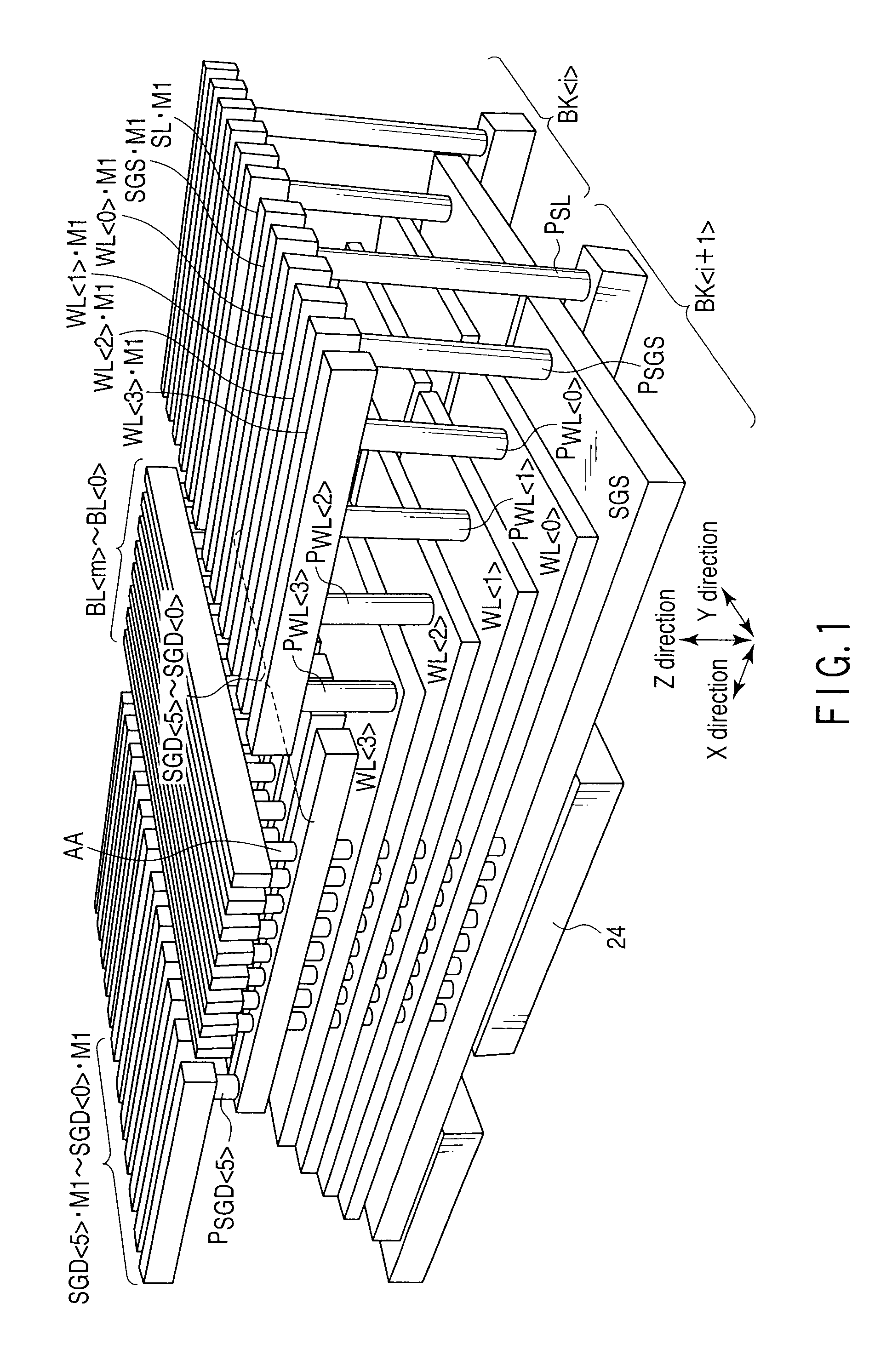
[0133]FIG. 13 shows a conceptual view of a layout of a first embodiment. FIG. 14 shows a plane layout when the conceptual view of FIG. 13 is specifically arranged as a device.

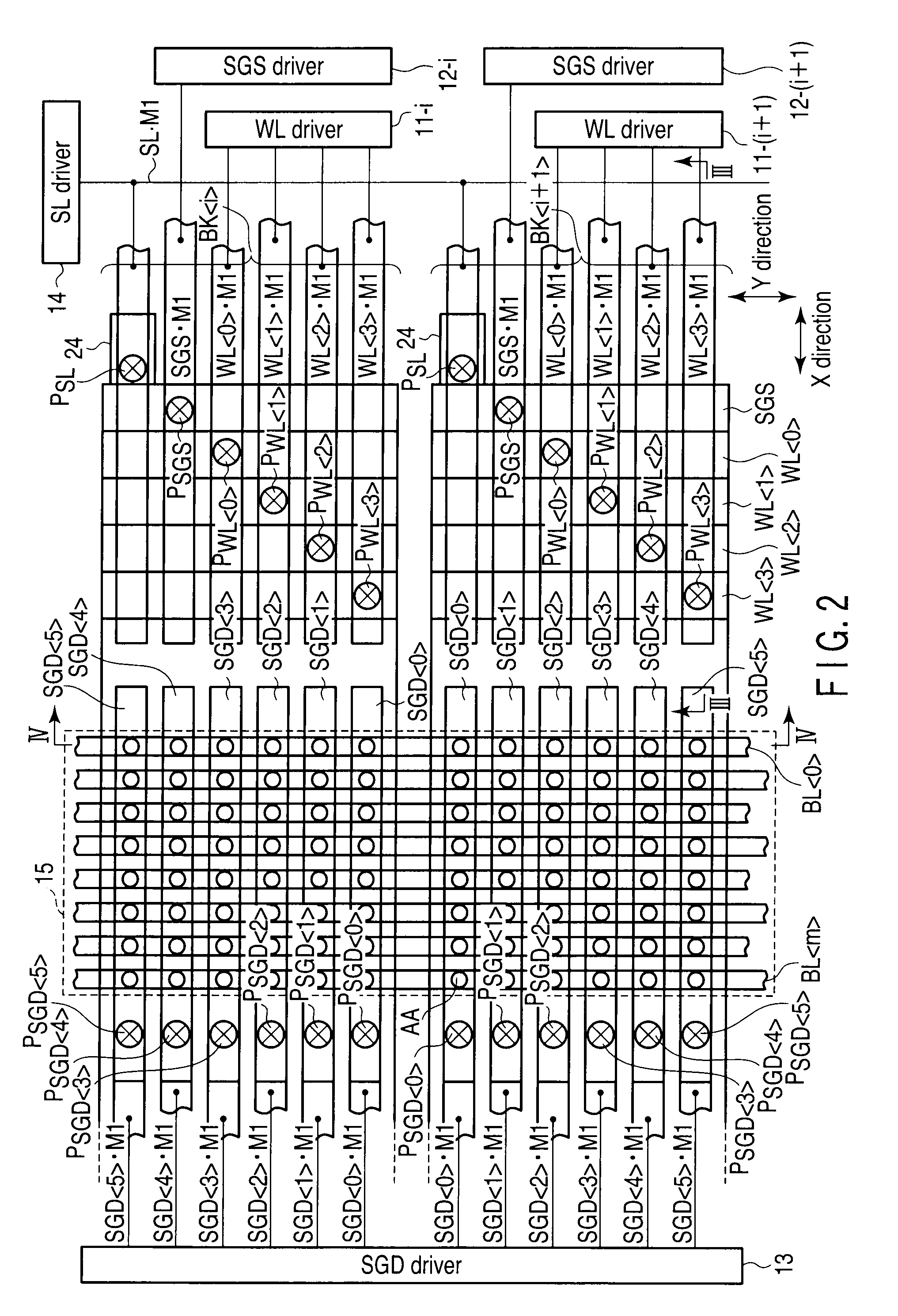
[0134]The first embodiment corresponds to the block layout of FIG. 9. That is, a driver 33L connected to select gate lines SGD0>, . . . , SGD5> on a bit line side is disposed on one end (left side) of a memory cell array 31 in the X-direction as well as disposed independently of a driver 33R connected to word lines WL0>, . . . , WL3> and to a select gate line SGS on a source line side.

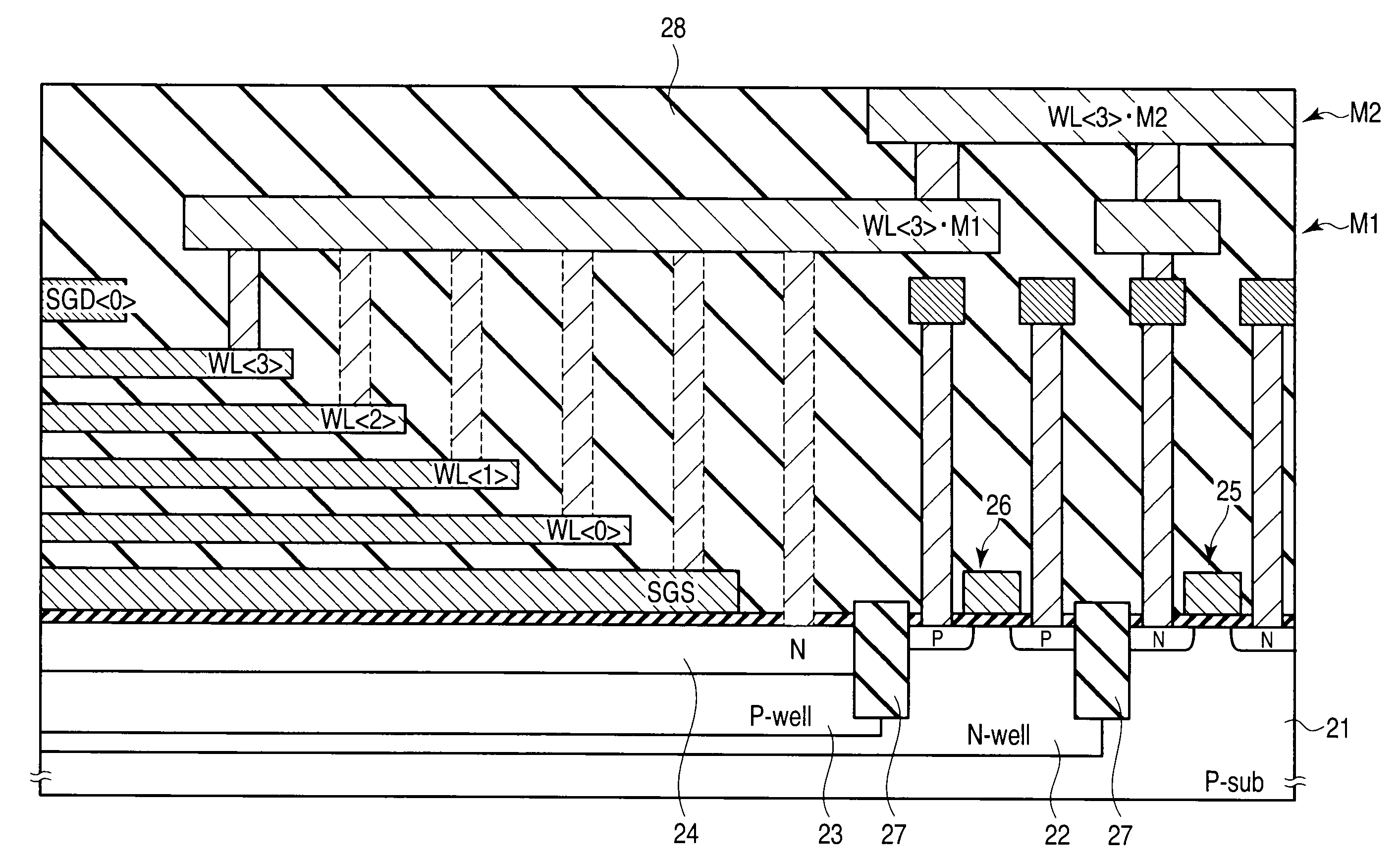
[0135]Each of two blocks BK, BK is comprised of at least three conductive layers, which are insulated from each other and stacked on a semiconductor substrate, bit lines BL0>, . . . , BL, which are insulated from the at least three conductive layers and disposed thereon, and active layers (columnar semiconductors) AA whose lower ends are connected to the semiconductor substrate, whose upper ends are connected to...

second embodiment

B. Second Embodiment

[0153]FIG. 15 shows a conceptual view of a layout of a second embodiment. FIG. 16 shows a plane layout when the conceptual view of FIG. 15 is specifically arranged as a device.

[0154]The second embodiment corresponds to the block layout of FIGS. 10 to 12. That is, a driver 33 (33L and 33R) disposed on one end (right side) of a memory cell array 31 in the X-direction is connected to word lines WL0>, . . . , WL3>, a select gate line SGS on a source line side, and select gate lines SGD0> . . . , SGD5> on a bit line side.

[0155]Attention must be paid to the fact that the portions, to which the layouts of FIGS. 15 and 16 are applied as they are, are limited to the portion between the memory cell array 31L and the driver 33L of FIG. 11 and to the portion between the memory cell array 31L and the driver 33 of FIG. 12.

[0156]The layouts, which are obtained by reversing the layouts of FIGS. 15 and 16 in a right to left direction, are applied to the remaining portions between...

first modification

A. First Modification

[0193]FIG. 24 shows a layout of a shunt area according to a first modification. FIG. 25 is a sectional view taken along line XXV-XXV of FIG. 24, and FIG. 26 is a sectional view taken along line XXVI-XXVI of FIG. 24.

[0194]The first modification has a feature in that a common source line STL•common is disposed above bit lines BL0>, . . . , BL and source lines STL and connected to the source lines STL.

[0195]Although the first modification is arranged based on the second embodiment (FIGS. 15 and 16), it can be also applied to the first embodiment (FIGS. 13 and 14) as a matter of course.

[0196]The common source line STL•common, which is connected to the source lines STL, is disposed above the bit lines BL0>, . . . , BL and the source lines STL. A layout of the common source line STL•common is not particularly limited. For example, the common source line STL•common may be formed flat on a memory cell array 31 or may be a conductive wire having a width larger than those...


PUM


Abstract

A three dimensional stacked nonvolatile semiconductor memory according to an example of the present invention includes a memory cell array comprised of first and second blocks disposed side by side in a first direction, and a driver disposed on one end of the memory cell array in a second direction orthogonal to the first direction. A source diffusion layer, which is common to the first and second blocks, is disposed in a semiconductor substrate, and a contact plug, which has a lower end connected to the source diffusion layer and an upper end connected to a source line disposed above at least three conductive layers, is interposed between the first and second blocks.

Description

CROSS-REFERENCE TO RELATED APPLICATIONS[0001]This application is based upon and claims the benefit of priority from prior Japanese Patent Application No. 2008-112658, filed Apr. 23, 2008, the entire contents of which are incorporated herein by reference.BACKGROUND OF THE INVENTION[0002]1. Field of the Invention[0003]The present invention relates to a three dimensional stacked nonvolatile semiconductor memory.[0004]2. Description of the Related Art[0005]BiCS (Bit Cost Scalable) technology is known as a technology for suppressing a bit cost of a semiconductor memory by increasing the capacity thereof by a three dimensional structure (refer to, for example, “Bit Cost Scalable Technology with Punch and Plug Process for Ultra High Density Flash Memory” 2007 Symposium on VLSI Technology Digest of Technical Papers. p. 14).[0006]A nonvolatile semiconductor memory to which the BiCS technology is applied (hereinafter, called a BiCS memory) has a feature in that it not only has a three dimensi...

Claims


Application Information

Patent Timeline
Patent Type & Authority Applications(United States)
IPC IPC(8): H01L29/788
CPCH01L27/11565H01L27/11582H01L27/11578H01L27/11573H01L2924/0002H10B43/10H10B43/20H10B43/40H10B43/27H01L2924/00H01L23/535H01L29/42344
Inventor MAEJIMA, HIROSHI
Owner KIOXIA CORP
Why Eureka
Try Eureka