

Liquid crystal display device
a liquid crystal display and liquid crystal technology, applied in the direction of thin material processing, instruments, chemistry apparatus and processes, etc., can solve the problems of difficult to maintain the controlled alignment of liquid crystal molecules for a long period, display unevenness, and difficult to stably control the alignment of liquid crystal molecules, etc., to achieve uniform distribution, prevent non-uniformity in the formation of polymer compounds, and control the effect of uniformity
- Summary
- Abstract
- Description
- Claims
- Application Information
AI Technical Summary
Benefits of technology
Problems solved by technology
Method used
Image

Examples
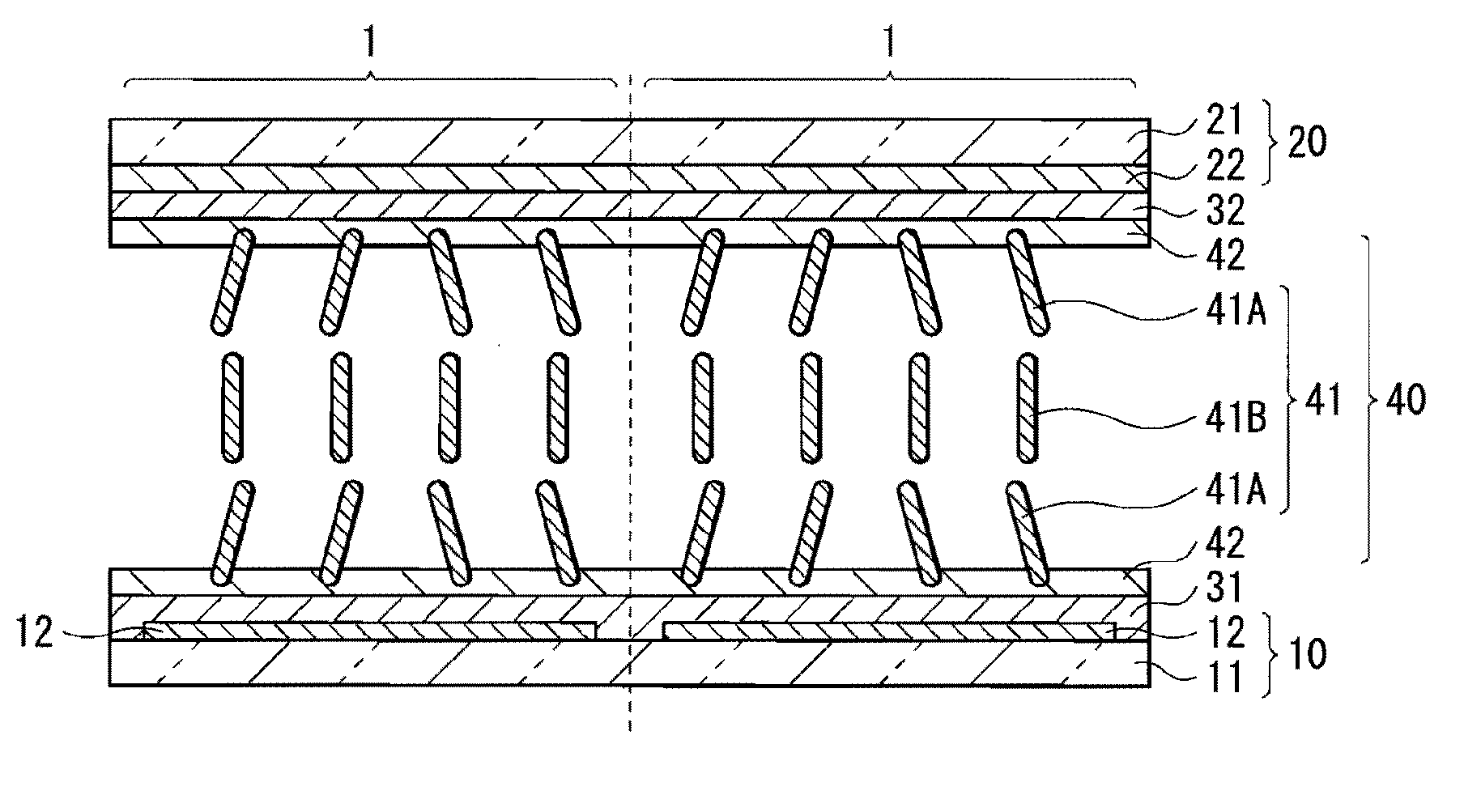
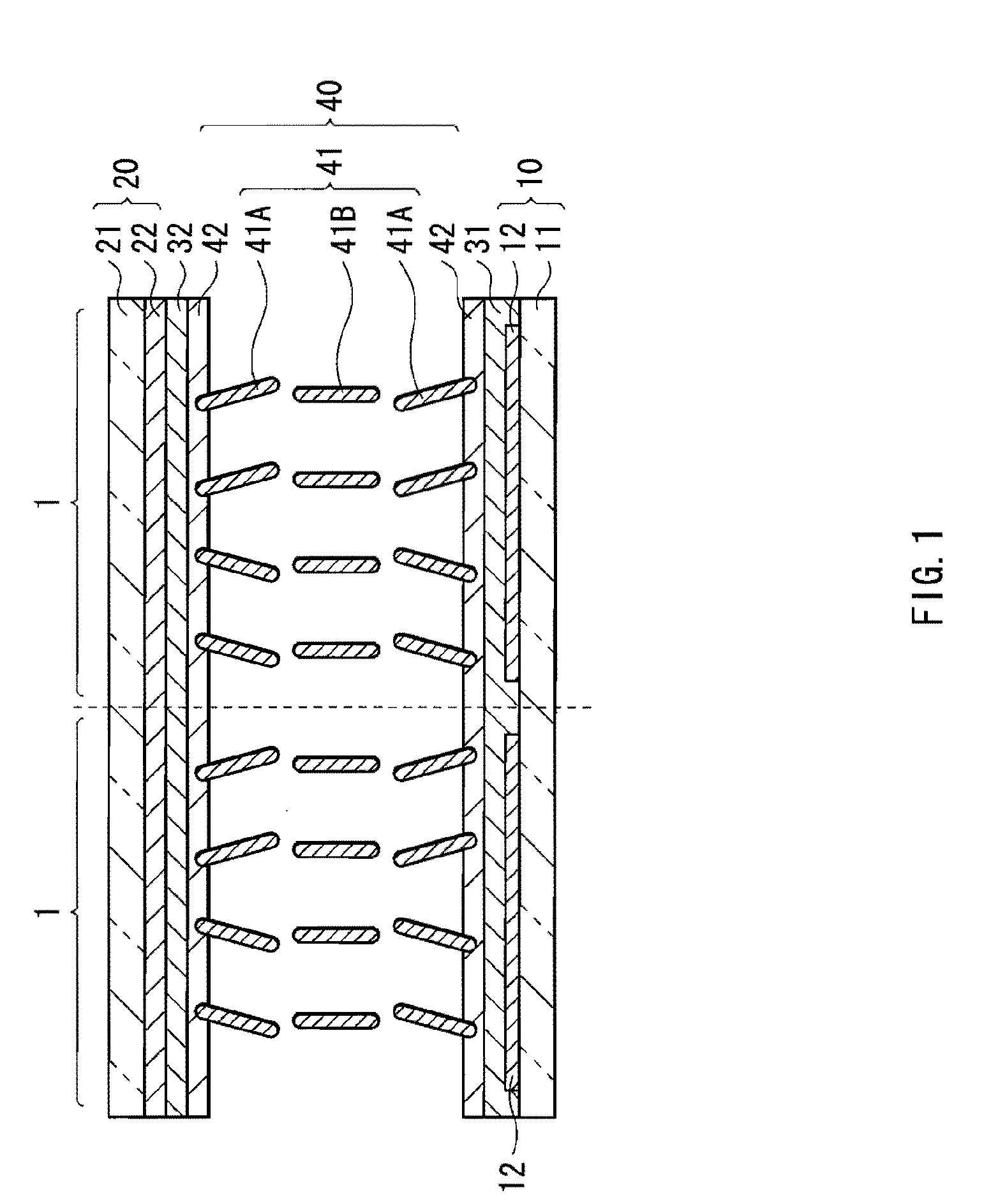
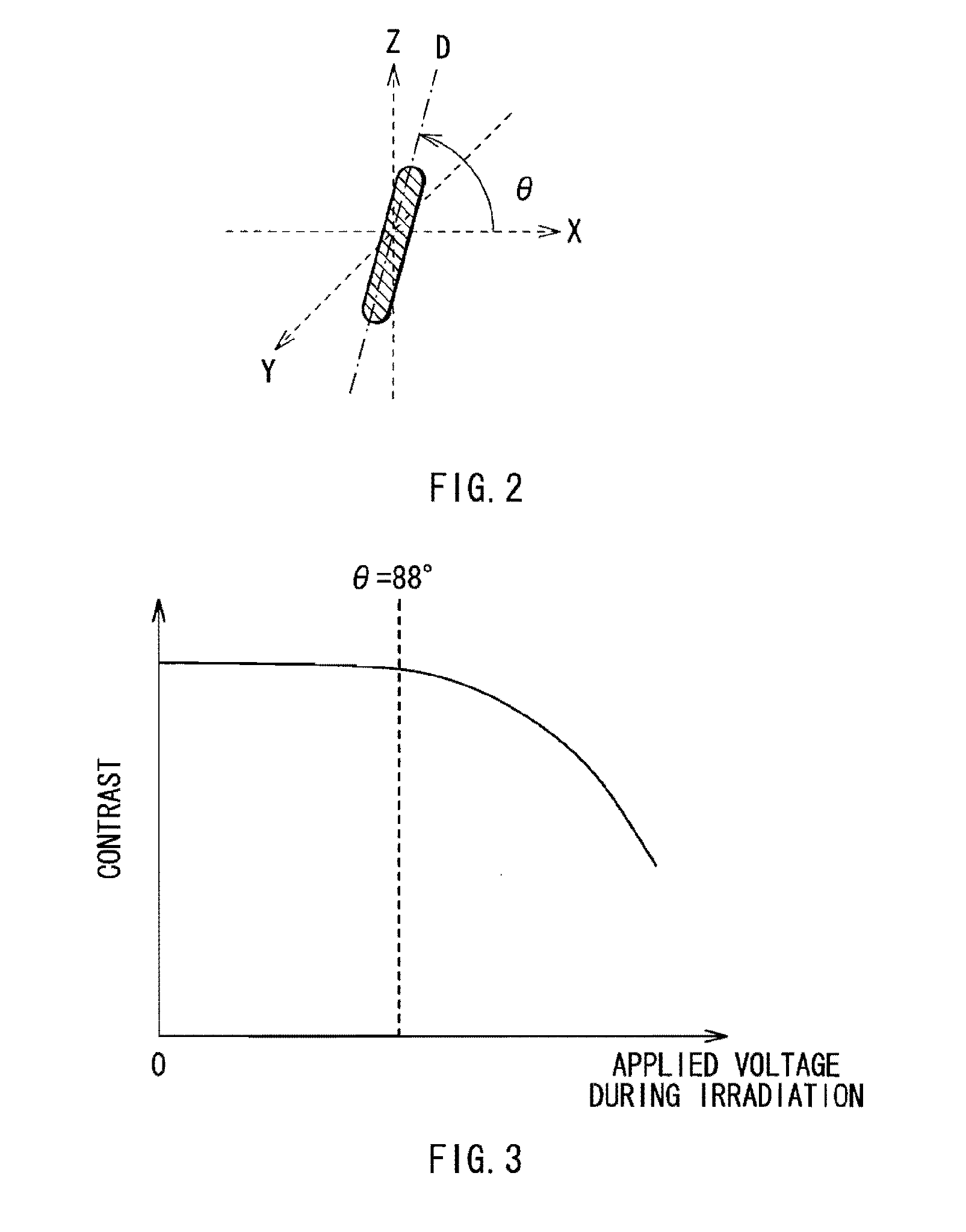
first embodiment
Modification of First Embodiment
[0061]FIG. 8 is a schematic sectional view of a liquid crystal display device according to a modification of the first embodiment, and FIGS. 9A and 9B are a schematic plan view of the common electrode 22 used in the liquid crystal display device illustrated in FIG. 8 and projections 24 arranged on the common electrode 22 (FIG. 9A) and a schematic plan view of a pixel electrode 14 (FIG. 9B). The liquid crystal display device has the same configuration as that of the liquid crystal display device according to the first embodiment except that the pixel electrode substrate 10 includes the pixel electrode 14 including a slit 14A, and the facing electrode substrate 20 includes the projections 24 on a surface on the liquid crystal layer 40 side of the common electrode 22.
[0062]The pixel electrode 14 includes the slit 14A so that 1 pixel is divided into a region 1A and a region 1B. The projections 24 are arranged between the alignment film 32 and the common e...
second embodiment
[0067]FIGS. 10A and 10B are schematic sectional views of a liquid crystal display device according to a second embodiment. FIG. 10A illustrates a state in which a drive voltage is not applied, and FIG. 10B illustrates a state in which a drive voltage is applied. The display mode of the liquid crystal display device illustrated in FIGS. 10A and 10B is a so-called IPS mode. For example, as illustrated in FIGS. 10A and 10B, the liquid crystal display device includes an electrode substrate 50 and a facing substrate 60 which face each other, alignment films 71 and 72 which are arranged so as to be laid over surfaces facing each other of the electrode substrate 50 and the facing substrate 60, and a liquid crystal layer 80 which is sealed between the electrode substrate 50 and the facing substrate 60 with the alignment films 71 and 72 in between, and the electrode substrate 50 has a configuration in which a pixel electrode 52 and a common electrode 53 are arranged. The liquid crystal displ...
third embodiment
[0083]FIGS. 11A and 11B are schematic sectional views of a liquid crystal display device according to a third embodiment. FIG. 11A illustrates a state in which a drive voltage is not applied, and FIG. 11B illustrates a state in which a drive voltage is applied. The display mode of the liquid crystal display device illustrated in FIGS. 11A and 11B is a so-called FFS mode. For example, as illustrated in FIGS. 11A and 11B, the liquid crystal display device includes an electrode substrate 100 and a facing substrate 110 which face each other, alignment films 121 and 122 which are arranged so as to be laid over surfaces facing each other of the electrode substrate 100 and the facing substrate 110, and a liquid crystal layer 130 which is sealed between the electrode substrate 100 and the facing substrate 110 with the alignment films 121 and 122 in between, and the electrode substrate 100 has a configuration in which a common electrode 102 and a pixel electrode 104 are arranged. The liquid ...
PUM
| Property | Measurement | Unit |
|---|---|---|
| dielectric constant | aaaaa | aaaaa |
| pretilt angle | aaaaa | aaaaa |
| pretilt angle | aaaaa | aaaaa |
Abstract
Description
Claims
Application Information