Opto-electronic package structure having silicon-substrate and method of forming the same

a technology of silicon-substrate and package structure, which is applied in the manufacture of printed circuits, solid-state devices, semiconductor devices, etc., can solve the problems of reducing the light intensity or failure of the entire device, the manufacturing process of electronic products is too complicated and tedious, and it is almost impossible to produce led packages b>10, etc., to achieve the effect of increasing the optical effect, simplifying the complexity of components, and great precision

Inactive Publication Date: 2009-11-05
TOUCH MICRO SYST TECH
View PDF21 Cites 282 Cited by
  • Summary
  • Abstract
  • Description
  • Claims
  • Application Information

AI Technical Summary

Benefits of technology

The present invention simplifies the design of an opto-electronic package by reducing the number of parts needed while improving its performance and reliability. This is achieved through precise production of silicon substrates that have various arrangements of components like connectors, opto-electronic devices, cups, and chips mounted on them. These improvements lead to better light coupling, improved cooling efficiency, and more reliable connections between components.

Problems solved by technology

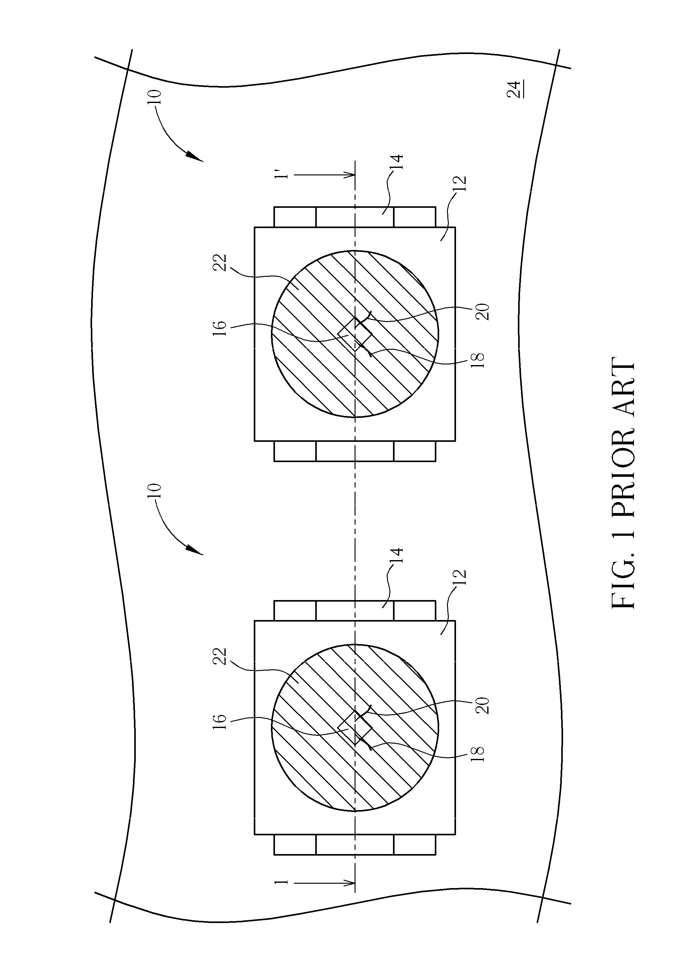
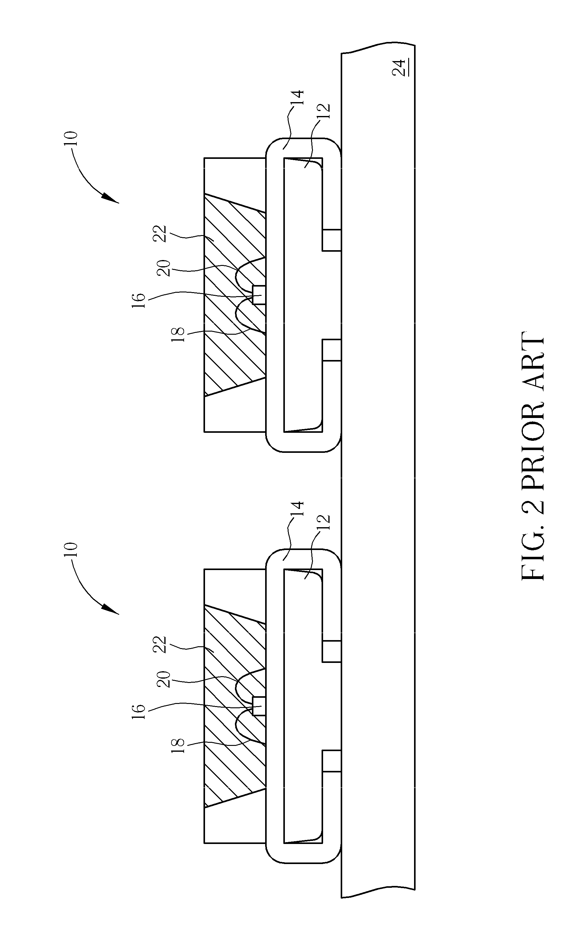
This patent discusses a problem related to current LED packaging structures, particularly those used in high-power applications like display screens and car headlights. Current methods require individual assembly of each LED package onto a circuit board, making them difficult to produce in bulk and leading to poor cooling performance that can reduce brightness or cause damage to sensitive parts. Additionally, there are limitations on design size due to the space needed for efficient heat dissipation. The technical problem addressed by this patent is how to create more efficiently produced and cooled LED packages suitable for use in these high-performance applications.

Method used


Image

  • Opto-electronic package structure having silicon-substrate and method of forming the same
  • Opto-electronic package structure having silicon-substrate and method of forming the same
  • Opto-electronic package structure having silicon-substrate and method of forming the same

Examples


Embodiment Construction

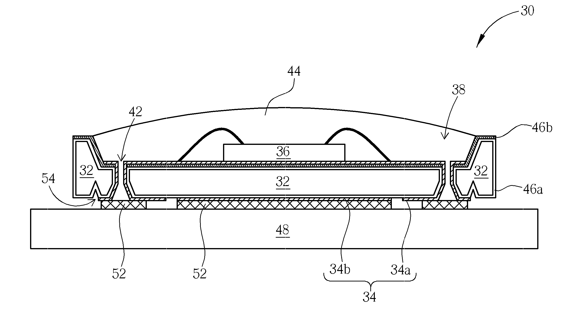
[0023]Please refer to FIG. 3 and FIG. 4. FIG. 3 is a schematic cross-sectional diagram illustrating an opto-electronic package structure 30 having a Si-substrate 32 according to a first preferred embodiment of the present invention, and FIG. 4 is a schematic top view of the opto-electronic package structure 30 shown in FIG. 3. It is to be understood that the drawings are not drawn to scale and are used only for illustration purposes. As shown in FIG. 3 and FIG. 4, an opto-electronic package structure 30 includes a Si-substrate 32, a plurality of connectors 34 and at least an opto-electronic device 36. The material of the Si-substrate 32 includes polysilicon, amorphous silicon or single-crystal silicon. In addition, the Si-substrate 32 can be a rectangle silicon chip or a circular silicon chip, and can include integrated circuits or passive components therein. The Si-substrate 32 has a top surface and a bottom surface. A cup-structure 38 can be included on the top surface of the Si-s...


PUM


Abstract

Disclosed herein is a structure of opto-electronic package having a Si-substrate. The Si-substrates are manufactured in batch utilizing the micro-electromechanical processes or the semiconductor processes, so that these Si-substrates are made with great precision and full of varieties. Based on the material characteristic of the Si-substrate, and the configuration of the components, such as the connectors, opto-electronic devices, depressions, solder bumps, etc., the present invention can improve the optical effect, the heat dissipating effect, and the reliability of the opto-electronic package structure, and simplifies the complexity of the opto-electronic package structure.

Description


Claims


Application Information

Patent Timeline
Owner TOUCH MICRO SYST TECH
Why Eureka
Try Eureka