Si-substrate and structure of opto-electronic package having the same

a technology of optoelectronic and substrate, which is applied in the manufacture of printed circuits, basic electric elements, solid-state devices, etc., can solve the problems of reducing the light intensity or failure of the entire device, the manufacturing process of electronic products is too complicated and tedious, and it is almost impossible to produce led packages b>10, etc., to achieve the effect of increasing the optical effect, simplifying the complexity of components, and great precision

Inactive Publication Date: 2008-01-24
TOUCH MICRO SYST TECH
View PDF13 Cites 0 Cited by
  • Summary
  • Abstract
  • Description
  • Claims
  • Application Information

AI Technical Summary

Benefits of technology

[0007]It is the primary object of the present invention to provide an opto-electronic package structure having a Si-substrate. Accordingly, the present invention can improve the optical effect, the heat dissipating effect, and the reliability of the opto-electronic package structure, the opto-electronic package structure can be manufactured in batch, and the complexity of the opto-electronic package structure can be simplified.
[0009]Since the Si-substrates can be produced in a batch system utilizing micro-electromechanical processes or semiconductor processes, these Si-substrates are made with great precision and full of varieties. According to the characteristics of Si-substrate and the arrangement of the components, such as the connecters, the opto-electronic device, the cup-structure and the flip-chip bump on Si-substrate, the present invention can simplify the complexity of the components in the opto-electronic package structure, and increase the optical effect, the heat-dissipating effect and the packaging reliability of the opto-electronic package structure.

Problems solved by technology

As a result, it is almost impossible to produce the LED packages 10 in batch, and the manufacturing process of the electronic products is too complicated and tedious.
As applied in a LED package 10 with high power, the cup-structure substrate 12 of the opto-electronic device 16 is unavoidably overheated, which may eventually result in a reduction of light intensity or failure of the entire device.
Due to the significantly large volume of the single LED package 10 and the heat radiating demand required by a LED package 10 with high power, the designed size and the heat dissipating efficiency of the whole LED package 10 are greatly limited.

Method used


Image

  • Si-substrate and structure of opto-electronic package having the same
  • Si-substrate and structure of opto-electronic package having the same
  • Si-substrate and structure of opto-electronic package having the same

Examples


Embodiment Construction

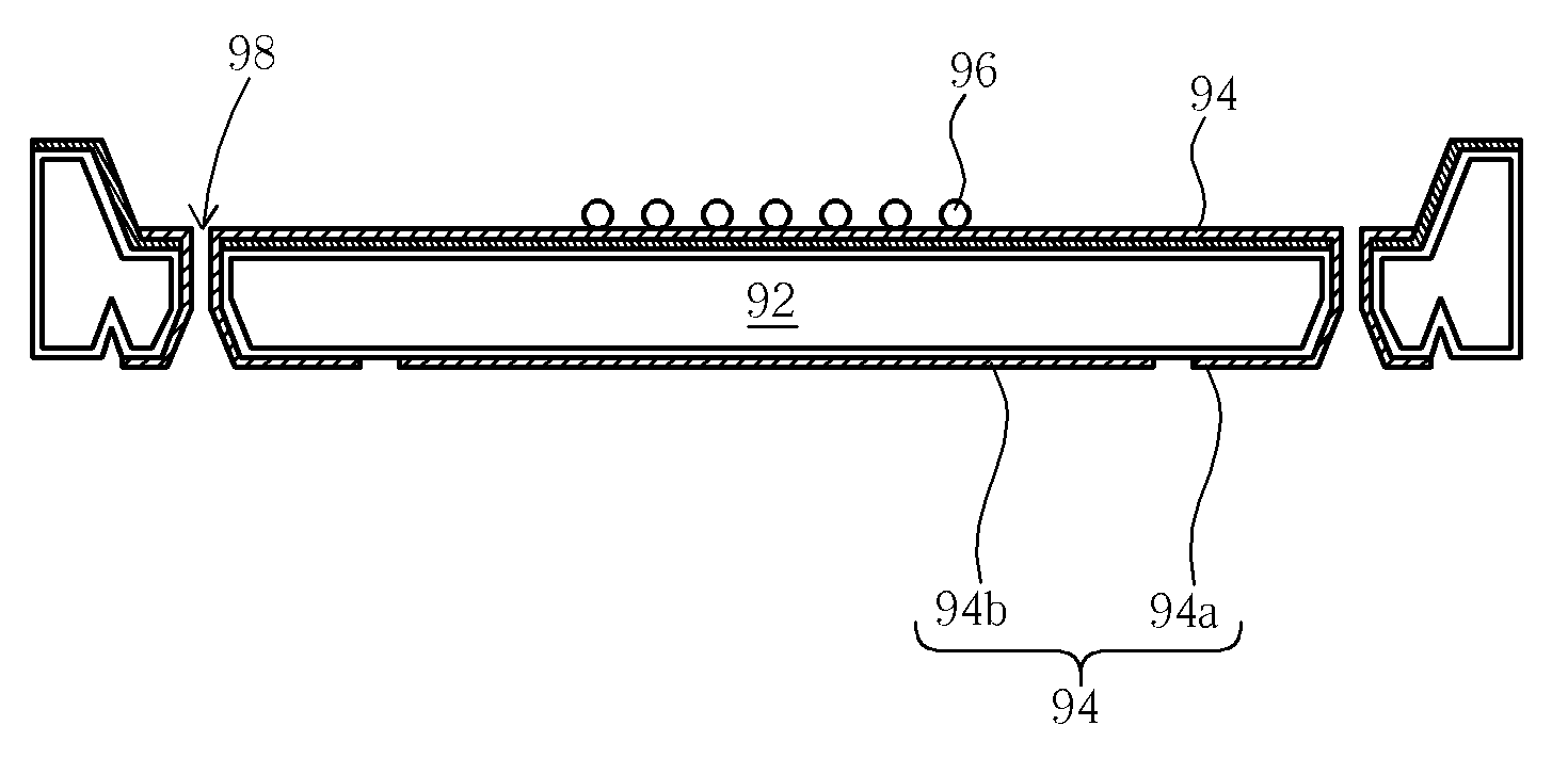
[0017]Please refer to FIG. 3. FIG. 3 is a cross-sectional schematic diagram illustrating a Si-substrate having flip-chip bumps according to a first preferred embodiment of the present invention. It is to be understood that the drawings are not drawn to scale and are served only for illustration purposes. As shown in FIG. 3, a Si-substrate 92 includes a plurality of connecters 94 and a plurality of flip-chip bumps 96. The Si-substrate 92 itself has a plurality of electric-conducting holes 98, and each electric-conducting hole 98 penetrates the Si-substrate 92 from the top surface to the bottom surface. The connecters 94 include a plurality of substrate-penetrating electric-conducting wires 94a and at least a heat-conducting wire 94b, and each substrate-penetrating electric-conducting wire 94 extends from the top surface of the Si-substrate 92 to the bottom surface of the Si-substrate 92 through the electric-conducting holes 98. The heat-conducting wire 94b covers parts of the bottom ...


PUM


Abstract

Disclosed herein is a structure of opto-electronic package having Si-substrate. The Si-substrates are manufactured in batch utilizing the micro-electromechanical processes or the semiconductor processes, so that these Si-substrates are made with great precision and full of varieties. Base on the material characteristic of the Si-substrate, and the configuration of the components, such as the connecters, opto-electronic devices, depressions, solder bumps, etc., the present invention can improve the optical effect, the heat dissipating effect, and the reliability of the opto-electronic package structure, and simplifies the complexity of the opto-electronic package structure.

Description

BACKGROUND OF THE INVENTION[0001]1. Field of the Invention[0002]The present invention generally relates to the field of opto-electronic package structures, and more particularly, to an opto-electronic package structure formed by the micro-electromechanical processes or the semiconductor processes.[0003]2. Description of the Prior Art[0004]In recent years, a new application field of high illumination light emitting diodes (LEDs) has been developed. Different from a common incandescent light, a cold illumination LED has the advantages of low power consumption, long device lifetime, no idling time, and quick response speed. In addition, since the LED also has the advantages of small size, vibration resistance, suitability for mass production, and ease of fabrication as a tiny device or an array device, it has been widely applied in display apparatuses and indicating lamps used in information, communication, and consumer electronic products. The LEDs are not only utilized in outdoor tra...

Claims


Application Information

Patent Timeline
Patent Type & Authority Applications(United States)
IPC IPC(8): H01L23/02H01L33/48H01L33/62H01L33/64
CPCH01L33/486H01L33/62H01L2924/10253H01L2224/48247H01L2924/01087H01L33/641H01L33/647H01L2224/48091H01L2224/48227H01L2924/01078H05K3/341H01L2924/00014H01L2924/00
Inventor LIN, HUNG-YI
Owner TOUCH MICRO SYST TECH
Why Eureka
Try Eureka