

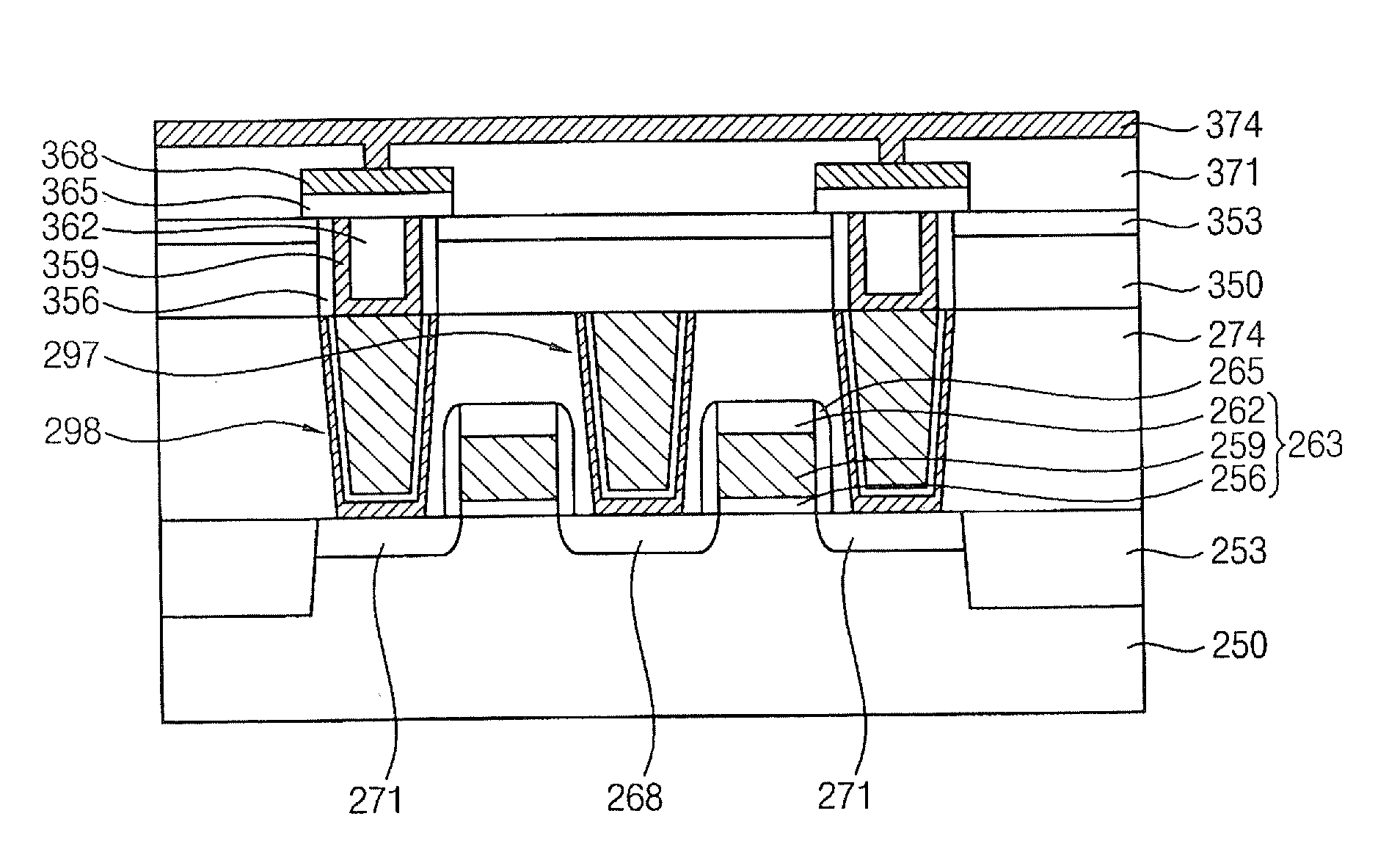
Method of forming a contact structure
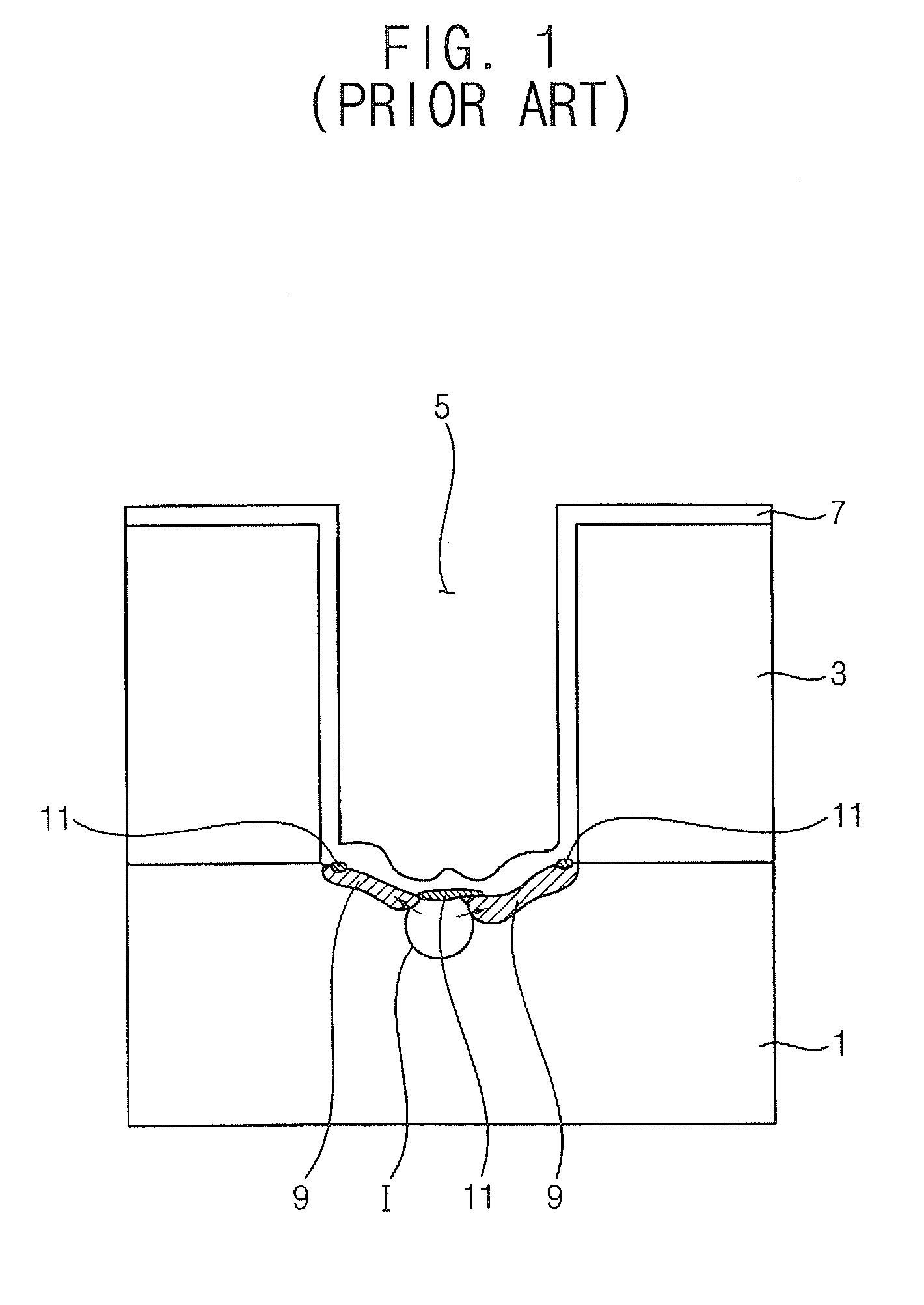
a contact structure and contact technology, applied in the direction of semiconductor devices, semiconductor/solid-state device details, electrical devices, etc., can solve the problems of metal silicide layer b>9/b> not being uniformly formed on the contact region, voids easily generated between the contact region,
- Summary
- Abstract
- Description
- Claims
- Application Information
AI Technical Summary
Benefits of technology
Problems solved by technology
Method used
Image

Examples
example 1
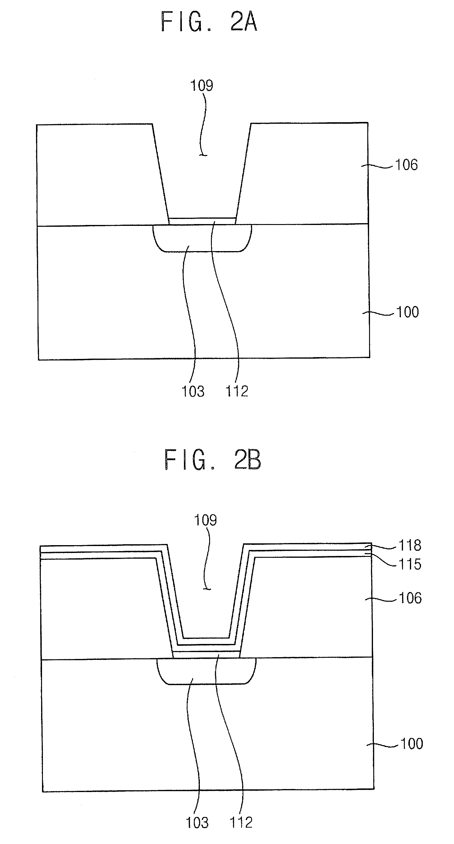
[0089]After forming a contact region on a substrate, an insulation layer was formed on the substrate. An opening exposing the contact region was formed through the insulation layer, and then a silicon oxide layer was formed on the contact region by providing an aqueous solution including diluted hydrofluoric acid, wherein a volume ratio of H2O and HF was about 1,000:1, and an aqueous solution having an ozone concentration of about 15 ppm for about 90 seconds onto the contact region of the substrate.
[0090]After a titanium layer was formed on the silicon oxide layer, a titanium oxide silicide layer was formed on the substrate by performing a silicidation process in which the silicon oxide layer was reacted with the titanium layer.
example 2
[0091]After forming a contact region on a substrate, an insulation layer was formed on the substrate. After forming an opening exposing the contact region through the insulation layer, a silicon oxide layer was formed on the contact region by providing an aqueous solution having an ozone concentration of about 25 ppm for about 150 seconds onto the contact region.
[0092]A titanium layer was formed on the silicon oxide layer, and then a titanium oxide silicide layer was formed on the contact region by performing a silicidation process in which the silicon oxide layer was reacted with the titanium layer.
example 3
[0093]A titanium oxide silicide layer was formed on a substrate through a process substantially the same as or substantially similar to that of Example 1, except that a silicon oxide layer was formed on a contact region of the substrate by providing an aqueous solution having an ozone concentration of about 35 ppm for about 80 seconds onto the contact region of the substrate.
PUM
 Abstract
Description
Claims
Application Information