Plasma display and method for driving plasma display panel

Inactive Publication Date: 2009-12-10
HITACHI CONSUMER ELECTRONICS CORP +1
View PDF5 Cites 2 Cited by
  • Summary
  • Abstract
  • Description
  • Claims
  • Application Information

AI Technical Summary

Benefits of technology

[0013]Aspects of the present invention provide a plasma display and a method for driving a plasma display pa

Problems solved by technology

The protective layer is damaged because high-voltage sustaining pulses are applied during the sustaining period and ions accumulate as the sustaining discharge is repeated.
This in turn increases th

Method used


Image

  • Plasma display and method for driving plasma display panel
  • Plasma display and method for driving plasma display panel
  • Plasma display and method for driving plasma display panel

Examples


first embodiment

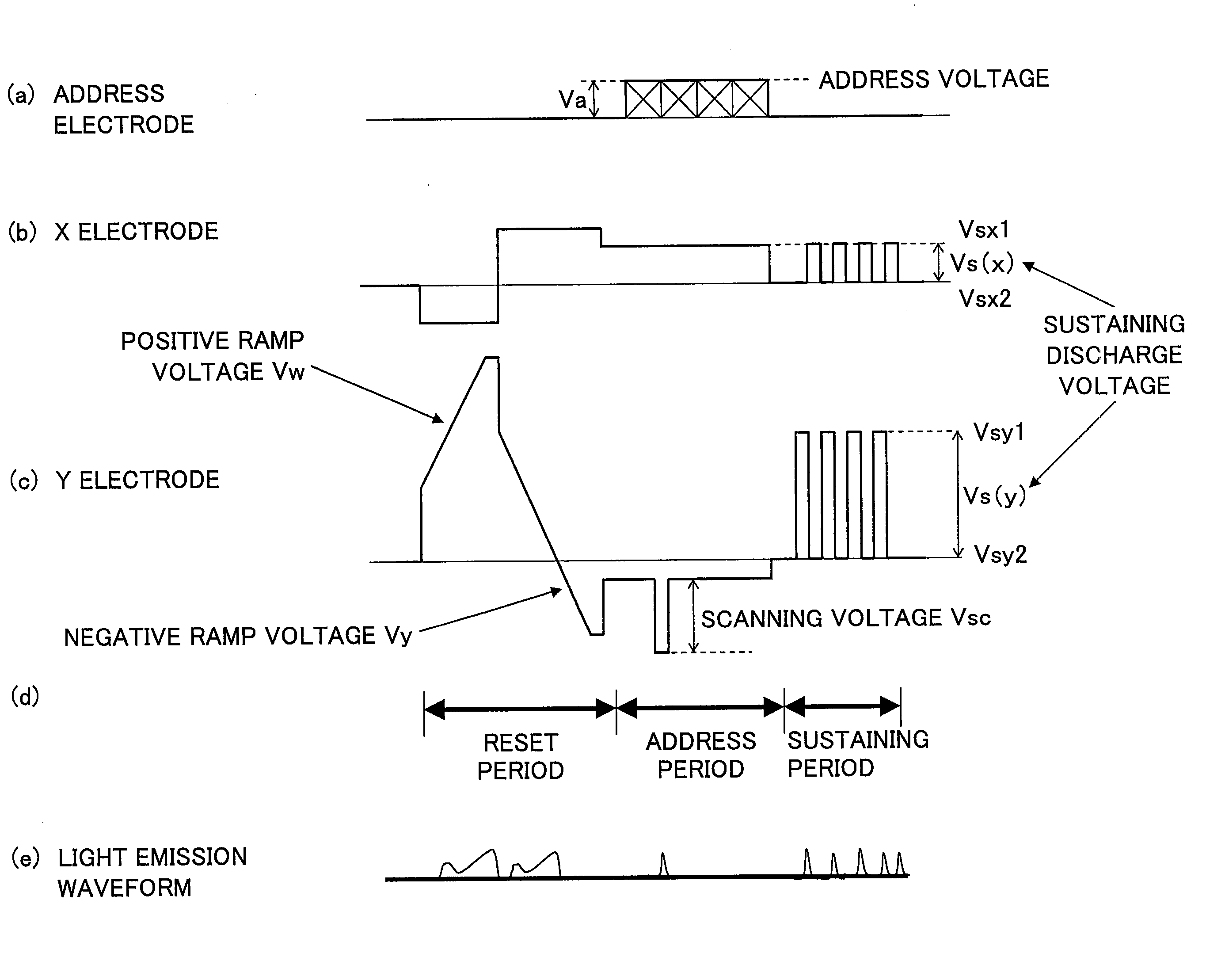
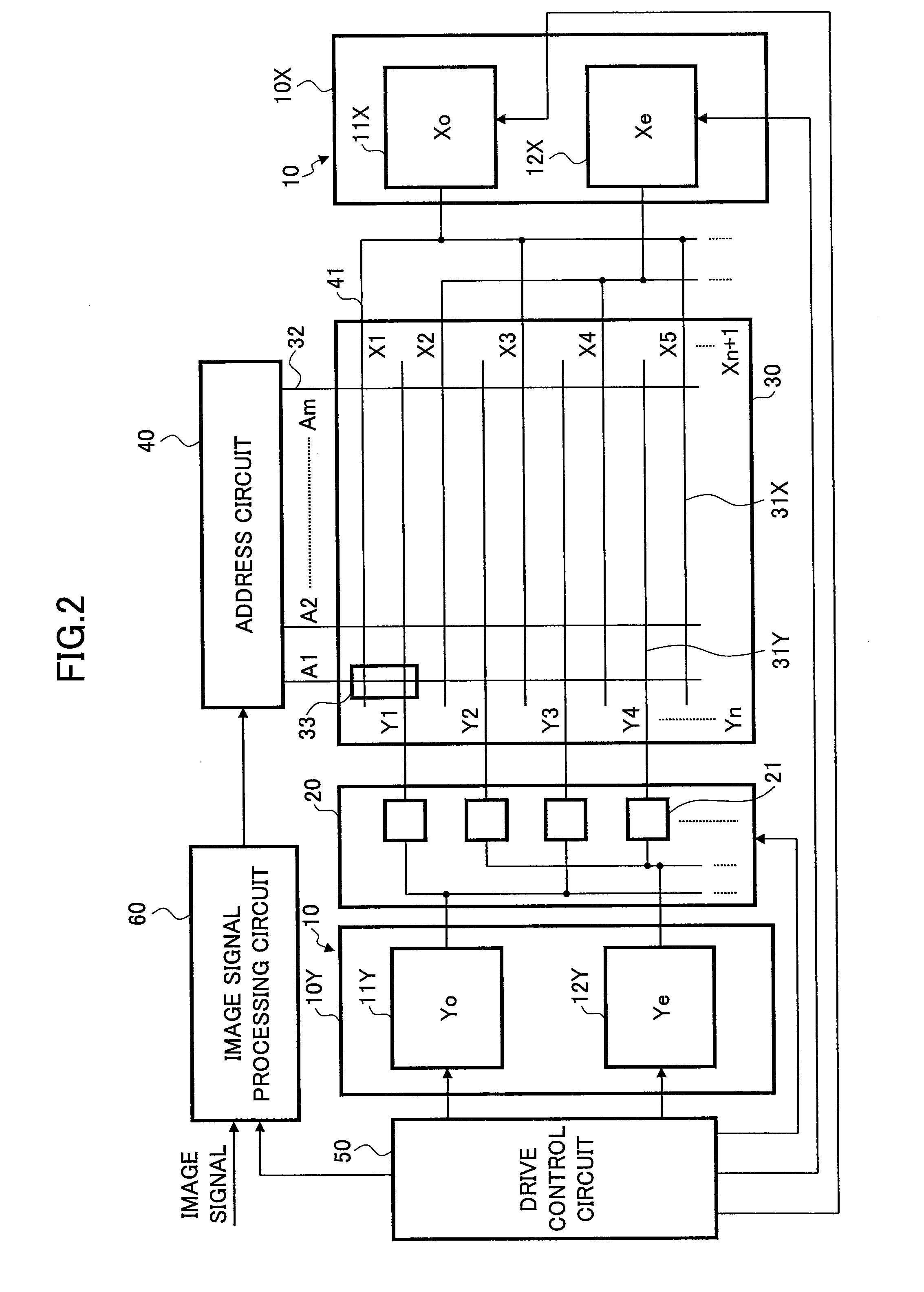
[0032]FIG. 2 is a schematic diagram illustrating a configuration of a plasma display according to a first embodiment of the present invention. A plasma display of this embodiment includes electrode driving circuits 10 including a Y-electrode driving circuit 10Y and an X-electrode driving circuit 10X, a scanning circuit 20, a plasma display panel (PDP) 30, an address circuit 40, a drive control circuit 50, and an image signal processing circuit 60.

[0033]The PDP 30 is a display panel for displaying an image and has a configuration based on the ALIS method described above. The PDP 30 includes “n” Y electrodes 31Y and “n+1” X electrodes 31X that are arranged parallel to each other in the horizontal direction and arranged alternately in the vertical direction. The PDP 30 also includes address electrodes 32 that are orthogonal to the Y electrodes 31Y and the X electrodes 31X. Thus, the electrodes are arranged to form a matrix. Display cells 33 are formed at intersections of the Y electrod...

second embodiment

[0067]FIG. 5 is a drawing illustrating examples of driving waveforms applied to the display electrodes (the X electrode 31X and the Y electrode 31Y) and operation timings of switches in a plasma display and a plasma display panel driving method according to a second embodiment of the present invention. In the plasma display and the plasma display panel driving method of the second embodiment, a low-voltage sustaining pulse is applied to the X electrode 31X as in the first embodiment. In the second embodiment, however, the width of the low-voltage sustaining pulse is changed such that the low-voltage sustaining pulse starts to fall at a timing that is different from the first embodiment with respect to the high-voltage sustaining pulse output from the Y sustaining circuit 11Y, 12Y and sustaining discharge occurs at different timings. The general configuration of the plasma display of this embodiment is substantially the same as that of the first embodiment shown in FIG. 3 and therefo...

third embodiment

[0074]FIG. 6 is a drawing illustrating examples of driving waveforms applied to the display electrodes (the X electrode 31X and the Y electrode 31Y) and operation timings of the switches SW1x through SW4x and SW1y through SW4y in a plasma display and a plasma display panel driving method according to a third embodiment of the present invention. Similar to FIG. 4 of the first embodiment, FIG. 6 (a) shows a driving voltage waveform of the X electrode 31X and FIG. 6 (b) shows a driving voltage waveform of the Y electrode 31Y. FIG. 6 (c) shows a potential difference obtained by subtracting an electric potential of the Y electrode 31Y from an electric potential of the X electrode 31X. FIG. 6 (d) shows a light emission waveform of the display cell 33. FIG. 6 (e) shows operation timings of the switches SW1x through SW4x of the X sustaining circuit 11X, 12X. FIG. 6 (f) shows operation timings of the switches SW1y through SW4y of the Y sustaining circuit 11Y, 12Y.

[0075]In the second embodime...


PUM


Abstract

A disclosed plasma display includes a plasma display panel including cells and display electrodes including a group of X electrodes and a group of Y electrodes; an X electrode driving circuit configured to apply a sustaining pulse to the group of X electrodes; and a Y electrode driving circuit configured to apply a sustaining pulse to the group of Y electrodes. One of the X electrode driving circuit and the Y electrode driving circuit applies a low-voltage sustaining pulse that can cause the sustaining discharge by itself to a corresponding one of the group of X electrodes and the group of Y electrodes. The other one of the X electrode driving circuit and the Y electrode driving circuit applies a high-voltage sustaining pulse that can cause the sustaining discharge by itself to the other one of the group of X electrodes and the group of Y electrodes.

Description

BACKGROUND OF THE INVENTION[0001]1. Field of the Invention[0002]A certain aspect of the present invention relates to a plasma display and a method for driving a plasma display panel.[0003]2. Description of the Related Art[0004]Plasma displays have become widely used as alternatives of cathode ray tube (CRT) displays. Plasma displays are self-luminous and therefore provide good visibility, are capable of displaying information at high speed, and are suitable for applications such as a thin display with a large screen. Display methods of plasma displays include a non-interlaced (progressive) method where all display lines are displayed in one field and an interlace method where an odd field displaying odd display lines and an even field displaying even display lines are displayed alternately.[0005]For example, Japanese Patent Application Publication No. 2004-309983 discloses an interlace method called an alternate lighting of surface (ALIS) method. In related-art plasma displays, each...

Claims


Application Information

Patent Timeline
IPC IPC(8): G09G3/28G09G5/00G09G3/20G09G3/288G09G3/291G09G3/292G09G3/294G09G3/296G09G3/298G09G3/299
CPCG09G3/2965G09G3/294
Inventor IMURA, HISAFUMIYAMAMOTO, KENICHI
Owner HITACHI CONSUMER ELECTRONICS CORP
Why Eureka
Try Eureka