Semiconductor integrated circuit, system device including semiconductor integrated circuit, and semiconductor integrated circuit control method

a technology of semiconductor integrated circuits and integrated circuits, which is applied in the direction of radio frequency controlled devices, memory adressing/allocation/relocation, instruments, etc., can solve the problems of increased production and testing costs of usb controllers, loss of programs in the ram, and availability of pre-installed programs at the factory

Inactive Publication Date: 2009-11-19
RICOH KK
View PDF7 Cites 2 Cited by
  • Summary
  • Abstract
  • Description
  • Claims
  • Application Information

AI Technical Summary

Benefits of technology

[0014]Embodiments of the present invention provide a semiconductor integrated circuit, a system device including the semiconductor integrated circuit, and a met

Problems solved by technology

One disadvantage of the USB controller 103 is that since the program ROM 111 is a read-only memory, only programs preinstalled at the factory are available.
However, adding an EPROM increases the production and testing costs of a USB controller.
Also, using a RAM instead of an EPROM causes another problem, since programs in the RAM are lost when power to the USB controller is cut off.
However, this method re

Method used


Image

  • Semiconductor integrated circuit, system device including semiconductor integrated circuit, and semiconductor integrated circuit control method
  • Semiconductor integrated circuit, system device including semiconductor integrated circuit, and semiconductor integrated circuit control method
  • Semiconductor integrated circuit, system device including semiconductor integrated circuit, and semiconductor integrated circuit control method

Examples


first embodiment

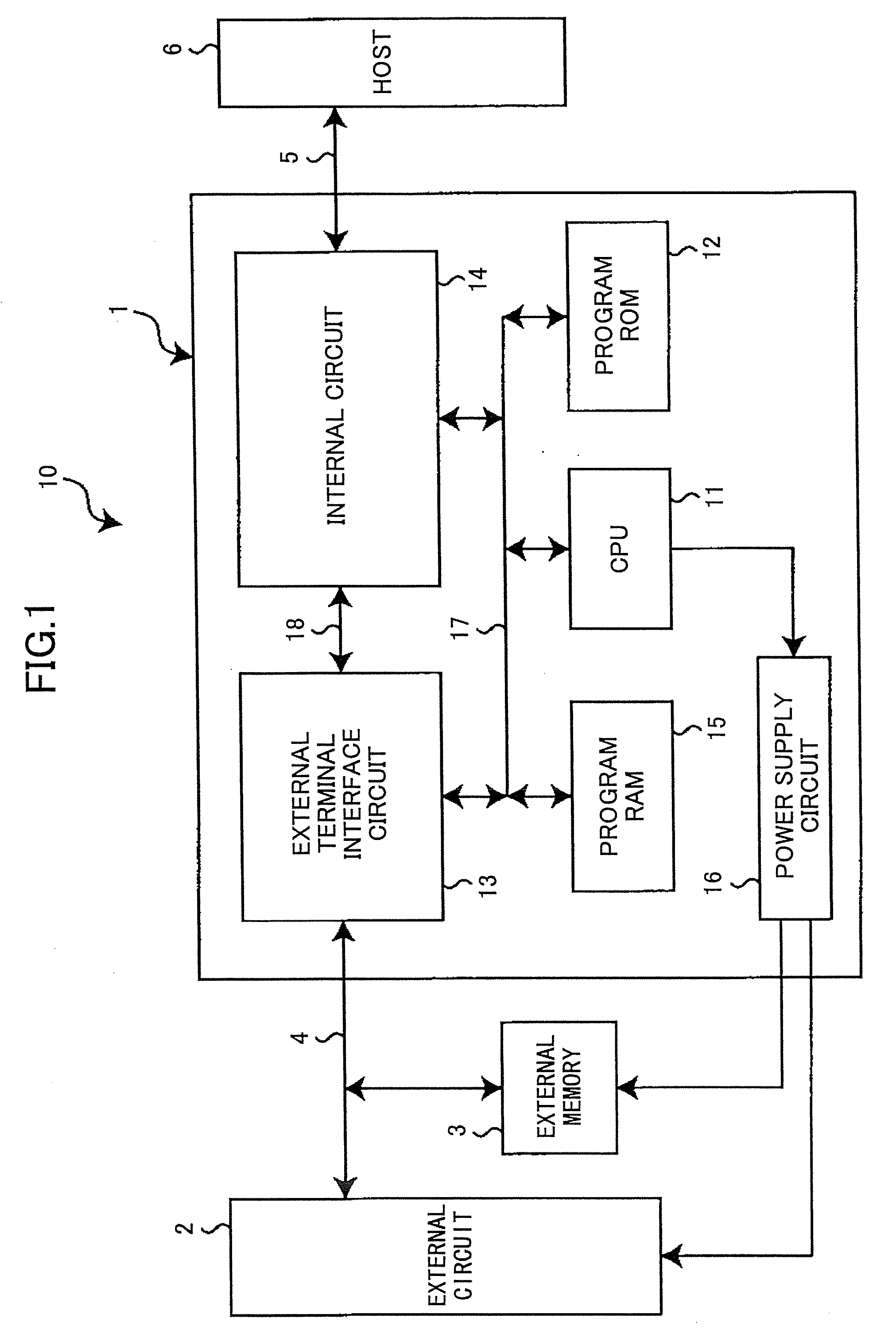
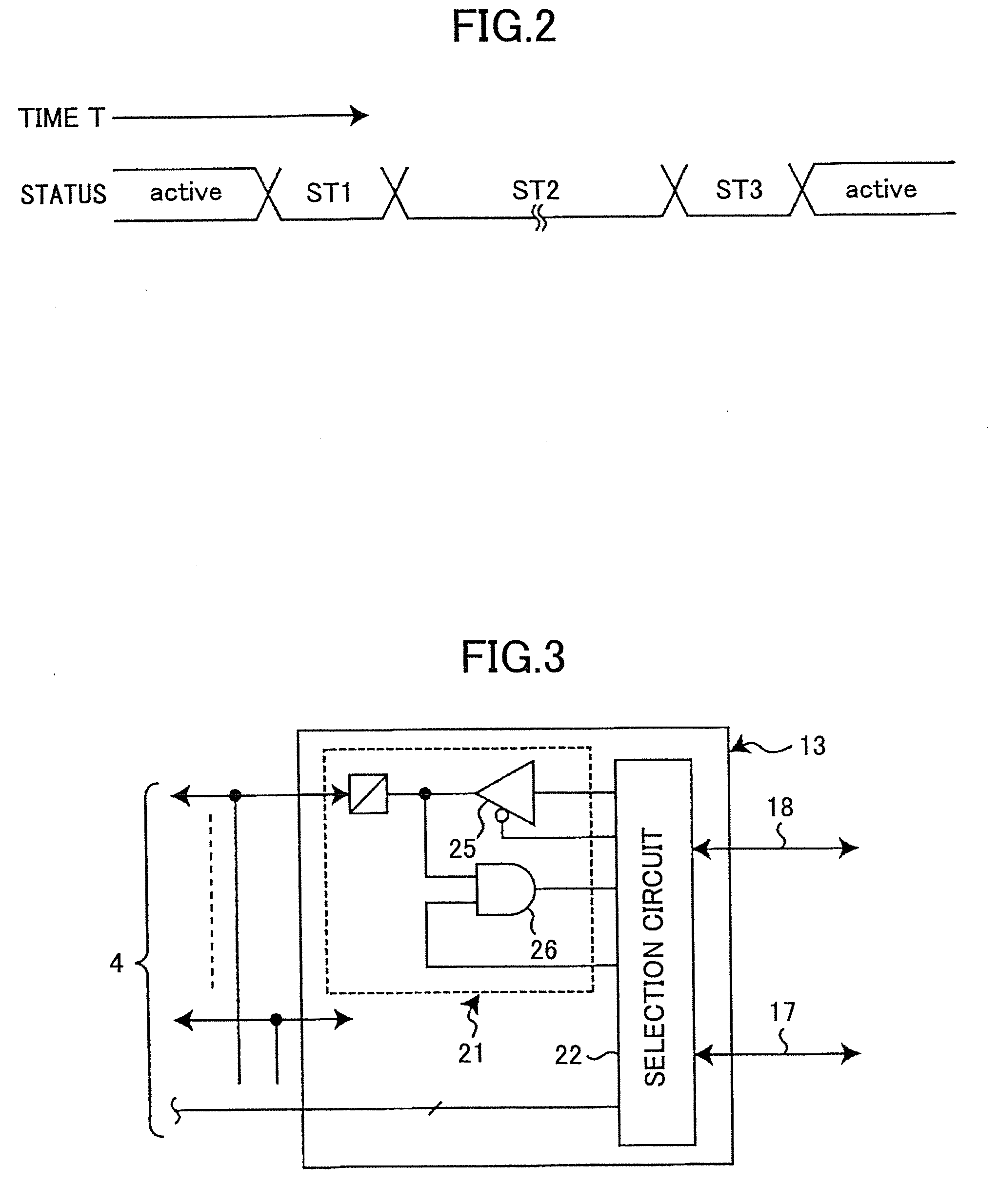
[0033]FIG. 1 is a block diagram illustrating an exemplary configuration of a system device 10 including a semiconductor integrated circuit 1 according to a first embodiment of the present invention.

[0034]As shown in FIG. 1, the system device 10 includes the semiconductor integrated circuit 1, an external circuit 2, and an external memory 3 that is a rewritable memory such as an EPROM. The semiconductor integrated circuit 1 includes external terminals (not shown) for connecting signal lines. The external circuit 2 and the external memory 3 are connected in parallel by an external signal line group 4 comprising multiple signal lines connected to the corresponding external terminals.

[0035]For example, a data signal output from the semiconductor integrated circuit 1 to the external signal line group 4 enters the external circuit 2 or the external memory 3. The semiconductor integrated circuit 1 is also connected to a host 6 such as a personal computer (hereafter called a PC) via an exte...

second embodiment

[0070]The semiconductor integrated circuit 1 of the first embodiment described above is configured to be able to input / output signals from / to the external circuit 2 or the external memory 3 using the same external signal line group 4 by controlling power supply to the external circuit 2 and the external memory 3. In a second embodiment of the present invention, a semiconductor integrated circuit la is configured to be able to input / output signals from / to an external circuit 2a or an external memory 3a using the same external signal line group 4 by using control signals to control data input-output functions of the external circuit 2a and the external memory 3a.

[0071]FIG. 9 is a block diagram illustrating an exemplary configuration of a system device 10a including the semiconductor integrated circuit 1a according to the second embodiment of the present invention. Components in FIG. 9 that correspond to those shown in FIG. 1 are assigned the same reference numbers and descriptions of...


PUM


Abstract

A disclosed semiconductor integrated circuit interfaces an external circuit and a host for controlling the external circuit and obtains data used to interface the external circuit and the host from a rewritable external memory. The disclosed semiconductor integrated circuit includes external terminals to which an external signal line group is connected, the external signal line group including signal lines connecting the external circuit and the external memory in parallel; an external terminal interface circuit configured to interface the semiconductor integrated circuit and the external circuit or the external memory connected via the external signal line group; and a control circuit configured to activate or deactivate the external circuit and the external memory. The control circuit is configured to activate either the external circuit or the external memory that is to be accessed via the external terminal interface circuit.

Description

TECHNICAL FIELD[0001]The present invention generally relates to a semiconductor integrated circuit used for a device such as a camcorder or a camera that includes, for example, a complementary metal-oxide semiconductor (CMOS) image sensor or a charge-coupled device (CCD) image sensor and is connectable to a parallel bus or a high-speed serial bus such as a universal serial bus (USB), a system device including the semiconductor integrated circuit, and a method of controlling the semiconductor integrated circuit.BACKGROUND ART[0002]In recent years, it has become very easy to hold a videoconference or to make a video-phone call using a camera including a CMOS sensor that is connectable via a USB to a personal computer (hereafter called a PC). This is largely due to development of small CMOS-sensor cameras (so called Web cameras) having high pixel counts and equipped with USB interfaces that are commonly used as general-purpose interfaces of PCs. Reducing the sizes of Web cameras is esp...

Claims


Application Information

Patent Timeline
IPC IPC(8): G06F12/00G06F12/02G11C5/14
CPCH01L27/14643H04N5/772H04N5/232H01L27/148G06F13/00G06F13/14
Inventor BABA, MITSUSHIGE
Owner RICOH KK
Why Eureka
Try Eureka