Printed circuit board and manufacturing method thereof

Inactive Publication Date: 2009-12-31
SAMSUNG ELECTRO MECHANICS CO LTD
View PDF3 Cites 2 Cited by
  • Summary
  • Abstract
  • Description
  • Claims
  • Application Information

AI Technical Summary

Benefits of technology

[0009]The invention provides a printed circuit board having a high efficien

Problems solved by technology

As passive components and packages loaded on the printed circuit board are increasing, there will be more heat generated, and electricity will be consumed more.
Thus, a quality of a printed circuit board may decrease.
However, a basic component of materials used for attachment mentioned above is mainly made of polymers, so that the heat transfer to the heat sinks may not be efficient enough.

Method used


Image

  • Printed circuit board and manufacturing method thereof
  • Printed circuit board and manufacturing method thereof
  • Printed circuit board and manufacturing method thereof

Examples


first embodiment

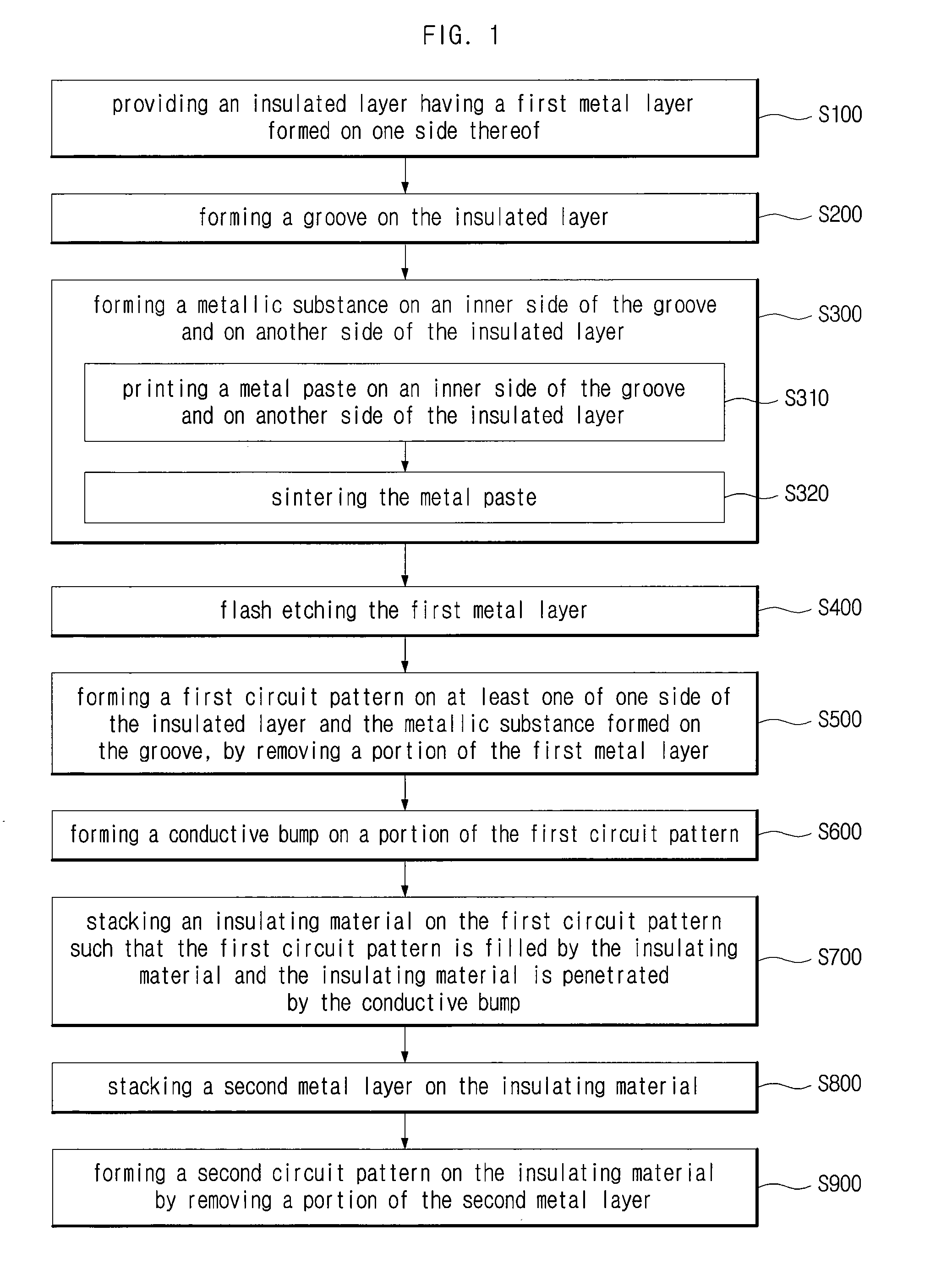
[0028]A method of manufacturing a printed circuit board in accordance with the present invention will be described below in detail with reference to the accompanying drawings.

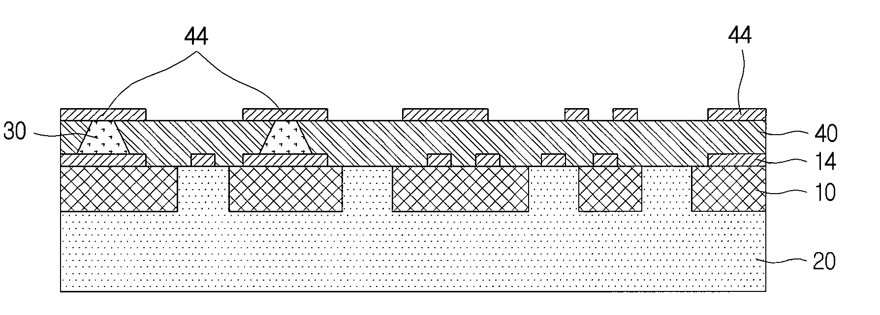
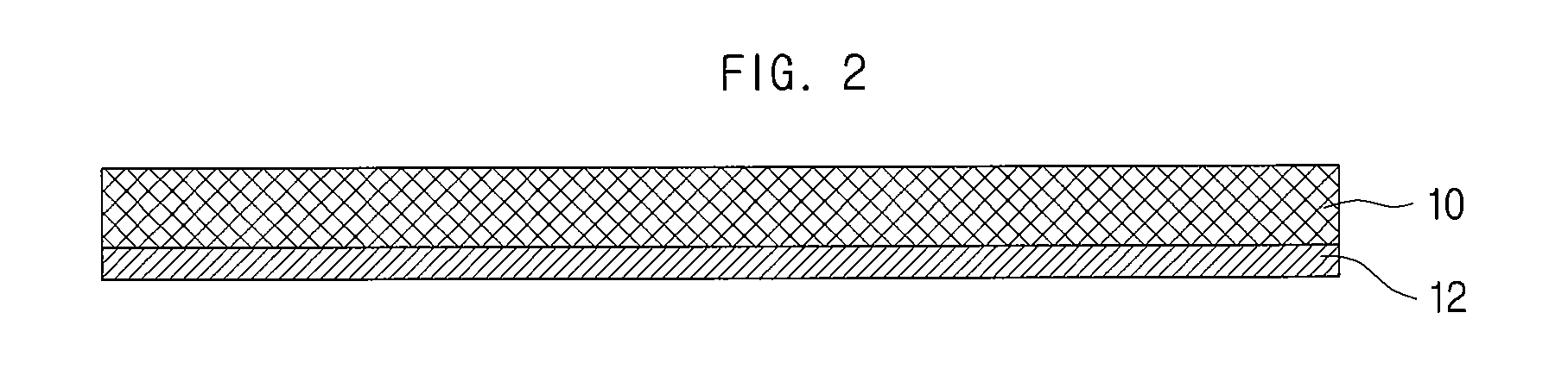
[0029]FIG. 1 is a flowchart illustrating a method of manufacturing a printed circuit board in accordance with a first embodiment of the present invention. FIGS. 2 to 11 are flowcharts illustrating a process of manufacturing a printed circuit pattern in accordance with a first embodiment of the present invention. Illustrated in FIGS. 2 to 11 are an insulated layer 10, a first metal layer 12, a first circuit pattern 14, a groove 16, a stamp 18, a metallic substance 20, a conductive bump 30, an insulating material 40, a second metal layer 42 and a second circuit pattern 44.

[0030]A first embodiment of the present invention, as illustrated in FIG. 2, provides an insulated layer 10 that has a first metal layer 12 formed on one side thereof (S100). The first metal layer 12 is made of a conductive metallic substance an...

second embodiment

[0055]Next, according to the present invention, each of multi-layered circuit patterns can be electrically connected by a conductive bump 30 and a via 60 in FIG. 13. That is, a first circuit pattern 14 and a second circuit pattern 44 are connected by the conductive bump 30 and the second circuit pattern 44 and a circuit pattern formed above it are connected by the via 60 as illustrated in FIG. 13.

third embodiment

[0056]Meanwhile, according to the present invention, multi-layered circuit patterns are electrically connected by a via 60.

[0057]That is, in other words, methods of electrically connecting the multi-layered circuit patterns can be varied by an intention of design and way of manufacturing.

[0058]The embodiments of the present invention as set forth above can provide the printed circuit board having a high efficiency of heat emission by disposing a heat sink in direct contact with a board and the method of manufacturing the printed circuit board.


PUM

PropertyMeasurementUnit
Electrical conductoraaaaaaaaaa
Metallic bondaaaaaaaaaa

Abstract

A printed circuit board and a method for manufacturing the printed circuit board are disclosed. The method can include; providing an insulated layer, in which a first metal layer is formed on one side of the insulated layer; forming a groove on the insulated layer; forming a metallic substance on an inner side of the groove and on another side of the insulated layer; and forming a first circuit pattern on at least one of one side of the insulated layer and the metallic substance formed on the groove by removing a portion of the first metal layer. The present invention provides the printed circuit board having a high efficiency of heat emission by disposing a heat sink in direct contact with a board and the method of manufacturing the printed circuit board.

Description

CROSS-REFERENCE TO RELATED APPLICATIONS[0001]This application claims the benefit of Korean Patent Application No. 10-2008-0060965 filed with the Korean Intellectual Property Office on Jun. 26, 2008, the disclosure of which is incorporated herein by reference in its entirety.BACKGROUND[0002]1. Technical Field[0003]The present invention relates to a printed circuit board and a method of manufacturing the printed circuit board.[0004]2. Description of the Related Art[0005]Recently, the demands have increased for a printed circuit board being loaded with a number of passive components and multi-layered high density packages, spurred by trends towards providing electronic equipments in thinner and smaller shape.[0006]A printed circuit board may connect or support electronic devices according to a type of circuit deigns desired by a designer. As passive components and packages loaded on the printed circuit board are increasing, there will be more heat generated, and electricity will be con...

Claims


Application Information

Patent Timeline
IPC IPC(8): H05K7/20H05K3/10
CPCB82Y10/00Y10T29/49126H05K1/056H05K1/183H05K3/005H05K3/4069H05K3/4608H05K3/4647H05K3/4652H05K2201/026H05K2201/0323H05K2201/0355H05K2201/0394H05K2203/0108H05K2203/1131Y10T29/49155Y10T29/49158Y10T29/49128Y10T29/49165Y10T29/4913H05K1/0206
Inventor HWANG, JUN-OHMOK, JEE-SOOPARK, JUN-HEYOUNGLEE, KYUNG-AHLEE, EUNG-SUEK
Owner SAMSUNG ELECTRO MECHANICS CO LTD
Why Eureka
Try Eureka