Plasma display panel apparatus driving method and plasma display panel apparatus

Inactive Publication Date: 2010-01-21
PANASONIC CORP
View PDF6 Cites 1 Cited by
  • Summary
  • Abstract
  • Description
  • Claims
  • Application Information

AI Technical Summary

Benefits of technology

[0023]According to the PDP apparatus and driving method for the same pertaining to the present invention, in at least one of the first section and second section, the potential of the first electrodes is changed to the above-described potential state, and the ramp waveform voltage is applied to the second electrodes either while the potential of the first electrodes is changing or at the above-described potential state. The set time of the ramp waveform portion (the time from the beginning of the change to the end of the change) is set longer than the time required for the potential of the first electrodes to reach the above-described potential. Therefore, according to the PDP apparatus and driving method for the same pertaining to the present invention, a stable weak discharge can be generated between the first electrodes and second electrodes in the section employing the method for setting the potential in the all-cell reset period, and this weak discharge is used as priming for generating a weak discharge between the first electrodes and third electrodes.
[0024]Also, according to the PDP apparatus and driving method for the same pertaining to the present invention, even when the ramp waveform voltage is applied to the second electrodes in the all-cell reset period, depending on the voltage value thereof, there are cases in which an opposing discharge is first generated between the second and third electrodes. However, since the second electrodes are cathodes and the third electrodes are anodes in the opposing discharge of the reset operation, this opposing discharge is more stable than an opposing discharge in which the third electrodes are cathodes. Therefore, according to the PDP apparatus and driving method for the same pertaining to the present invention, a stable reset discharge can be generated even with this type of discharge.
[0025]In the technology disclosed in patent document 2, an auxiliary erase pulse is applied after the all-cell

Problems solved by technology

However, in the driving of the PDP apparatus, issues in terms of image quality arise if there is simply a series of the subfields composed of a write period and a sustain period as described above, due to the remaining history of the wall charge of a previous subfield, and

Method used


Image

  • Plasma display panel apparatus driving method and plasma display panel apparatus
  • Plasma display panel apparatus driving method and plasma display panel apparatus
  • Plasma display panel apparatus driving method and plasma display panel apparatus

Examples


Example

Embodiment 1

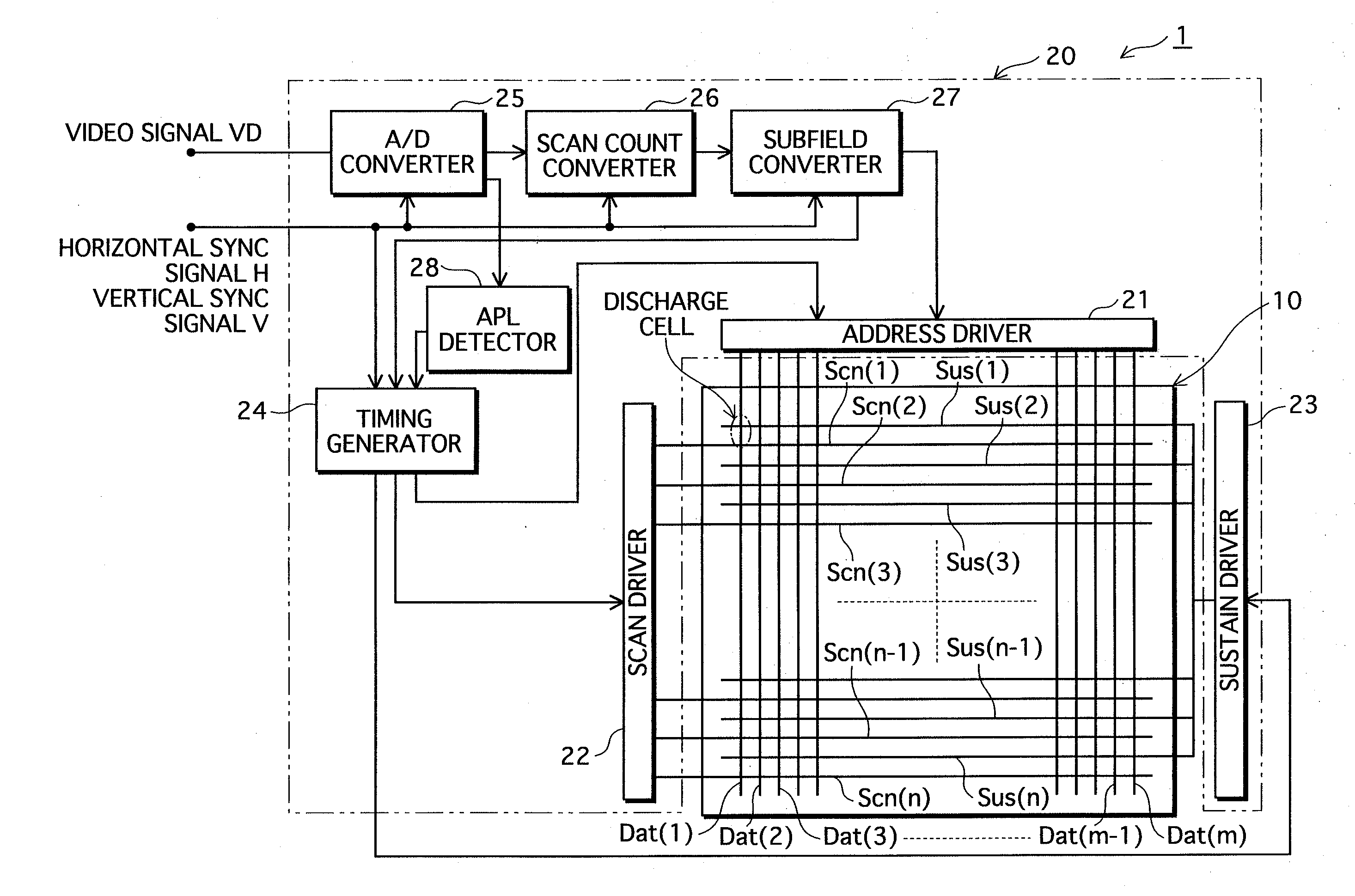
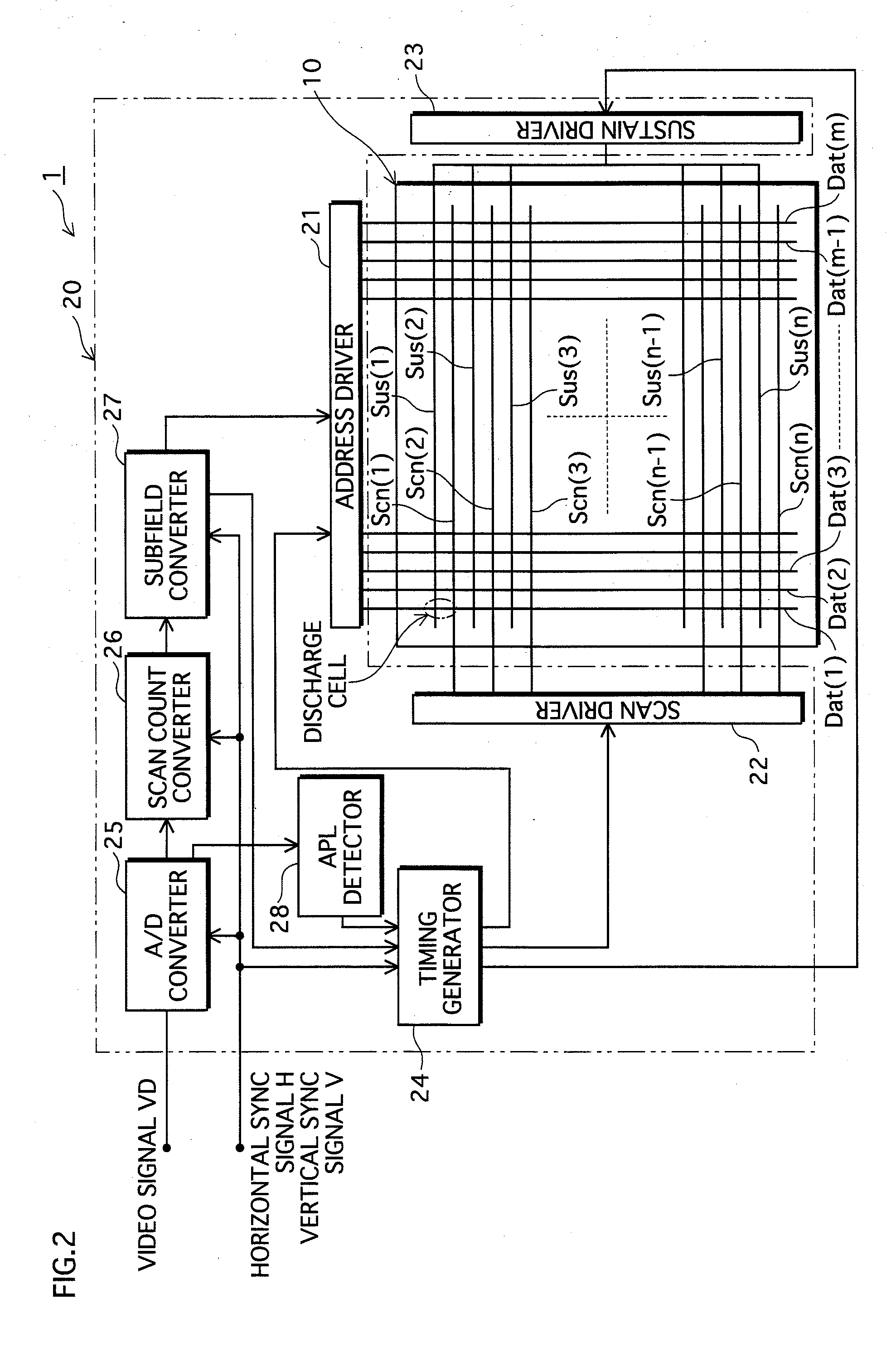
[0075]1. Structure of Panel Unit 10

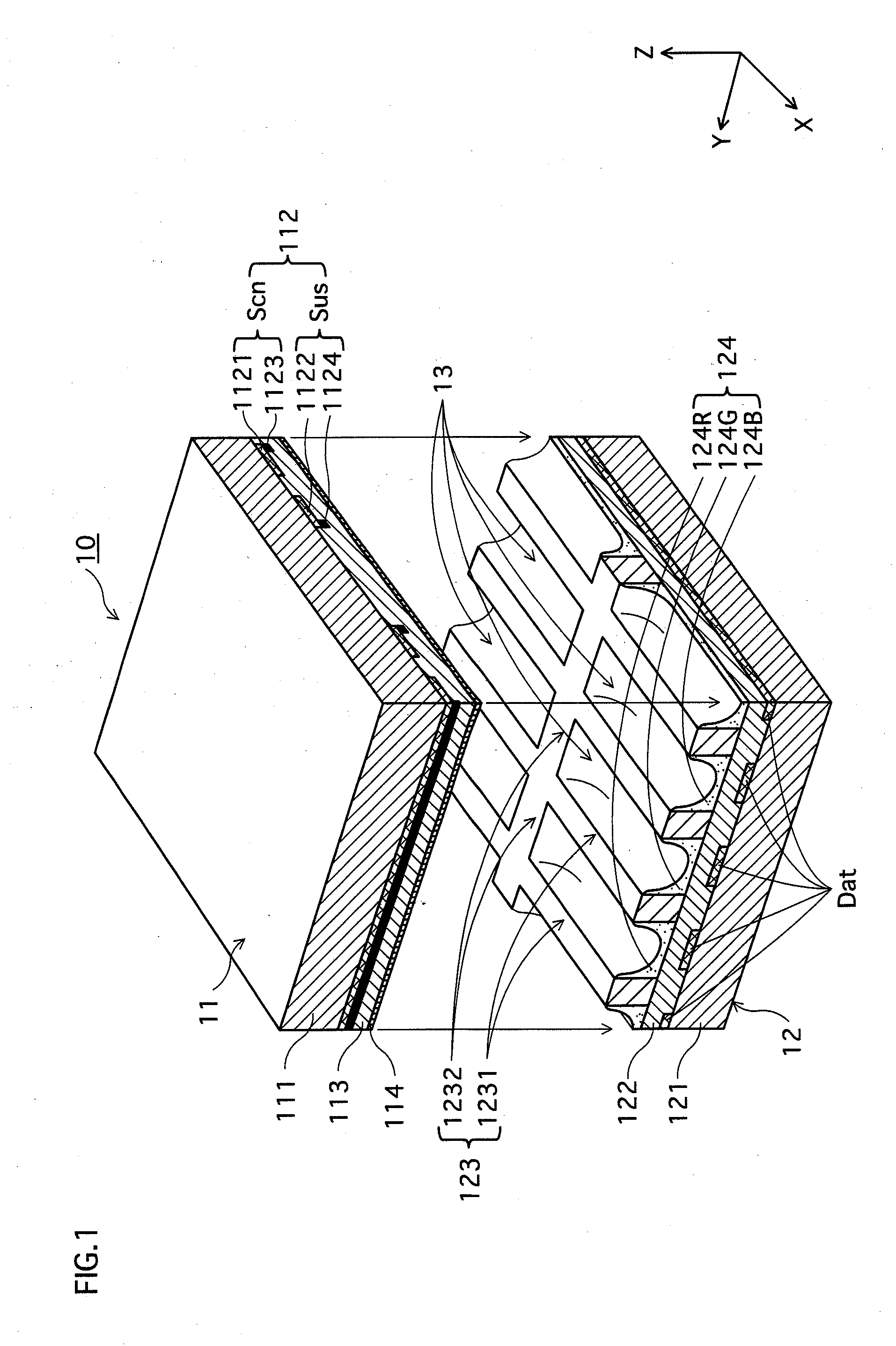
[0076]The structure of a panel unit 10, which is a portion of the structure of a PDP apparatus 1 pertaining to embodiment 1 of the present invention, is described below with reference to FIG. 1. FIG. 1 is a perspective view (partial cross-sectional view) showing a relevant portion of the structure of the panel unit 10 pertaining to embodiment 1.

[0077]As shown in FIG. 1, the panel unit 10 has a structure in which two panels 11 and 12 have been disposed in opposition with a discharge space 13 therebetween.

[0078]1-1. Structure of Front Panel 11

[0079]As shown in FIG. 1, a front panel 11 corresponding to the panel 11 constituting the panel unit 10 includes a front substrate 111, display electrode pairs 112 that are each composed of a scan electrode Scn and a sustain electrode Sus and that have been disposed in parallel on a surface (in FIG. 1, the bottom surface) of the front substrate 111 that faces a back panel 12 corresponding to the pane...

Example

Embodiment 2

[0200]The following describes a driving method for a PDP apparatus pertaining to embodiment 2, with reference to FIG. 10. FIG. 10 is a waveform diagram showing voltage waveforms applied to the electrodes Scn(1) to Scn(n), Sus(1) to Sus(n), and Dat(1) to Dat(m) in the all-cell reset period T6 in the driving method for the PDP pertaining to the present embodiment.

[0201]The PDP apparatus pertaining to the present embodiment has the same structure as the PDP apparatus 1, and the driving method for the same is the same as in embodiment 1, with the exception of the all-cell reset period T6, and descriptions thereof have therefore been omitted. The following description focuses on only the all-cell reset period T6 in the driving method.

[0202]As shown in FIG. 10, in the driving method pertaining to the present embodiment, the waveforms of the pulse Pul.1 applied to the scan electrodes Scn(1) to Scn(n) in the all-cell reset period T6 and the waveforms of the pulses Pul.2 and Pul....


PUM


Abstract

In a former half (T11) of an all-cell reset period (T1), the potential of a scan electrode (Scn) is raised from 0 [V] to Vp [V] at a timing t0, and thereafter maintained at the positive potential of Vp [V] to Vg [V] until a timing t3 when the former half (T11) ends. On the other hand, in the same former half (T11), a reset pulse (Pul.2), which includes a negative ramp waveform portion from 0 [V] to a potential of Vr [V], is applied to a sustain electrode (Sus). A time period (t1−t0) of the negative ramp waveform portion of the pulse (Pul.2) is set longer than a time period required for the potential change of a pulse (Pul.1) from P1 to P2.

Description

TECHNICAL FIELD[0001]The present invention relates to a plasma display panel apparatus and a driving method for the same, and in particular to technology for suppressing the generation of erroneous discharges in a reset period during driving.BACKGROUND ART[0002]A surface-discharge alternating-current type plasma display panel (hereinafter, simply called a “PDP”), which has currently become mainstream among various plasma display panels, has the following structure. In the PDP, two panels have been disposed in opposition to each other with an interval therebetween, an outer circumferential portion of the panels has been sealed, and a discharge gas that includes Xe has been filled into the interval. One of the two panels constituting the PDP (here, the front panel) includes a glass substrate having display electrode pairs (each including a scan electrode and a sustain electrode) formed on a main surface thereof, and a dielectric layer and a protective film that have been laminated the...

Claims


Application Information

Patent Timeline
IPC IPC(8): G06F3/038G09G3/28G09G3/288G09G3/291G09G3/292G09G3/298
CPCG09G3/2022G09G3/2927G09G2360/16G09G2320/0238G09G2310/066G09G3/292G09G3/296
Inventor AKAMATSU, KEIJIOGAWA, KENJIUEDA, MITSUO
Owner PANASONIC CORP
Why Eureka
Try Eureka