Imaging method and apparatus

a technology of image acquisition and image sensor, applied in the field of image acquisition method and apparatus, can solve the problems of large size and cost of such a system for acquiring images, difficulty in image matching of color images and depth images, and insufficient depth image matching, etc.

Active Publication Date: 2010-01-28
SAMSUNG ELECTRONICS CO LTD
View PDF11 Cites 128 Cited by
  • Summary
  • Abstract
  • Description
  • Claims
  • Application Information

AI Technical Summary

Benefits of technology

[0013]In an aspect of one or more embodiments, a size of the image sensor may be decreased using a pixel structure that a plurality of pixels share in a detecting circuit compared to a image sensor having sepa

Problems solved by technology

Such a beam-splitting approach requires the use of a beam splitter and typically more than two sensors, which generates size and cost problems.
Here, the size and cost of such a system for acquiring an image may be too large or high for a conventional camera application.
In addition, with such an arrangement, since the characteristics and required positioni

Method used


Image

  • Imaging method and apparatus
  • Imaging method and apparatus
  • Imaging method and apparatus

Examples


Embodiment Construction

[0045]Reference will now be made in detail to embodiments, examples of which are illustrated in the accompanying drawings, wherein like reference numerals refer to like elements throughout. In this regard, embodiments of the present invention may be embodied in many different forms and should not be construed as being limited to embodiments set forth herein. Accordingly, embodiments are merely described below, by referring to the figures, to explain aspects of the present invention.

[0046]FIG. 13 illustrates an image sensor 1300, according to one or more embodiments.

[0047]Referring to FIG. 13, the image sensor 1300 may include a plurality of pixels, such as pixel 1310, which is further illustrated in FIGS. 14-15.

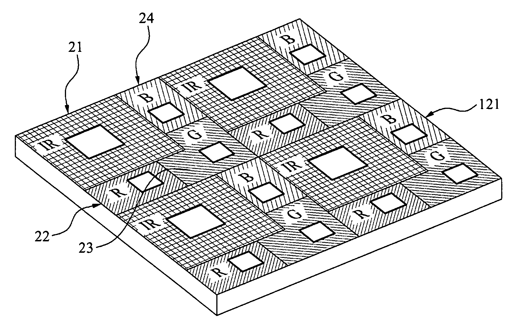
[0048]The plurality of pixels may constitute an array. For example, if a row includes 240 pixels and a column includes 320 pixels, the image sensor 1300 could be referenced to as having a 320×240 resolution. In this instance, this 320×240 resolution image sensor could be furt...


PUM


Abstract

Disclosed are an imaging method and apparatus. The apparatus may include an image sensor that may include a plurality of pixels, wherein at least one pixel of the plurality of pixels includes a light-detector element and a filter that band-passes a select visible light component to the light-detector element and band-passes a select non-visible light component to the light-detector element. A color value and depth value may be obtained using the same pixel through the image sensor.

Description

CROSS-REFERENCE TO RELATED APPLICATIONS[0001]This application claims the priority benefit of Korean Patent Application No. 10-2008-0072992, filed on Jul. 25, 2008 in the Korean Intellectual Property Office, the disclosure of which is incorporated herein by reference.BACKGROUND[0002]1. Field[0003]One or more embodiments relating to an imaging method and apparatus.[0004]2. Description of the Related Art[0005]Currently, portable devices having image sensors, such as digital cameras, mobile communication terminals, and the like, are being developed and marketed. These image sensors are made up by an array of small photodiodes referred to as pixels or photosites. In general, a pixel does not directly extract a particular color from received light, but converts a photon of a wide spectrum band into an electron or charge. Accordingly, the pixel of the image sensor may only need to receive light within a band necessary for obtaining or identifying a color from the light of the wide spectrum...

Claims


Application Information

Patent Timeline
IPC IPC(8): H04N5/335H01L27/14H01L27/146H04N5/369H04N5/374H04N9/07
CPCG01S17/89H04N3/155H04N5/335H04N5/37457H04N9/045H04N5/35545G01S17/894H04N25/581H04N25/778H04N25/131H04N25/134H04N25/136H04N25/00H04N23/12
Inventor KIM, SEONG JIN
Owner SAMSUNG ELECTRONICS CO LTD
Why Eureka
Try Eureka