

Epoxy Resin Composition for Optical-Semiconductor Encapsulation, Cured Resin Thereof, and Optical Semiconductor Device Obtained with the same
a technology of semiconductor devices and encapsulation, which is applied in the direction of semiconductor/solid-state device details, solid-state devices, organic dyes, etc., can solve the problems of colorant disadvantageously changing the optical property of shielding near infrared rays, low shielding ability of glass, and insufficient use in illuminance sensors. , to achieve the effect of reducing or eliminating the property of shielding, preventing optical properties, and changing the optical properties of colorants
- Summary
- Abstract
- Description
- Claims
- Application Information
AI Technical Summary
Benefits of technology
Problems solved by technology
Method used
Image

Examples
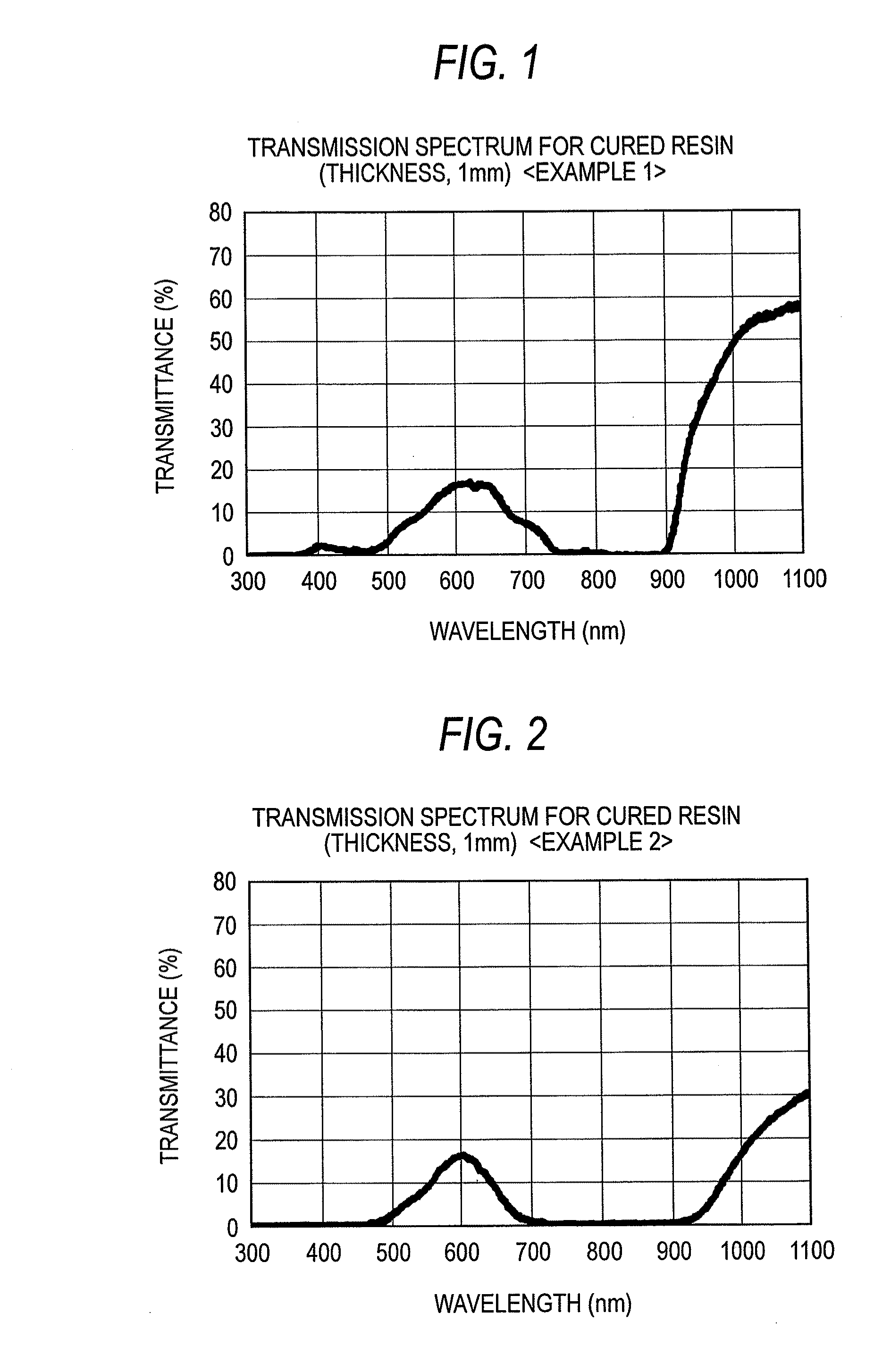
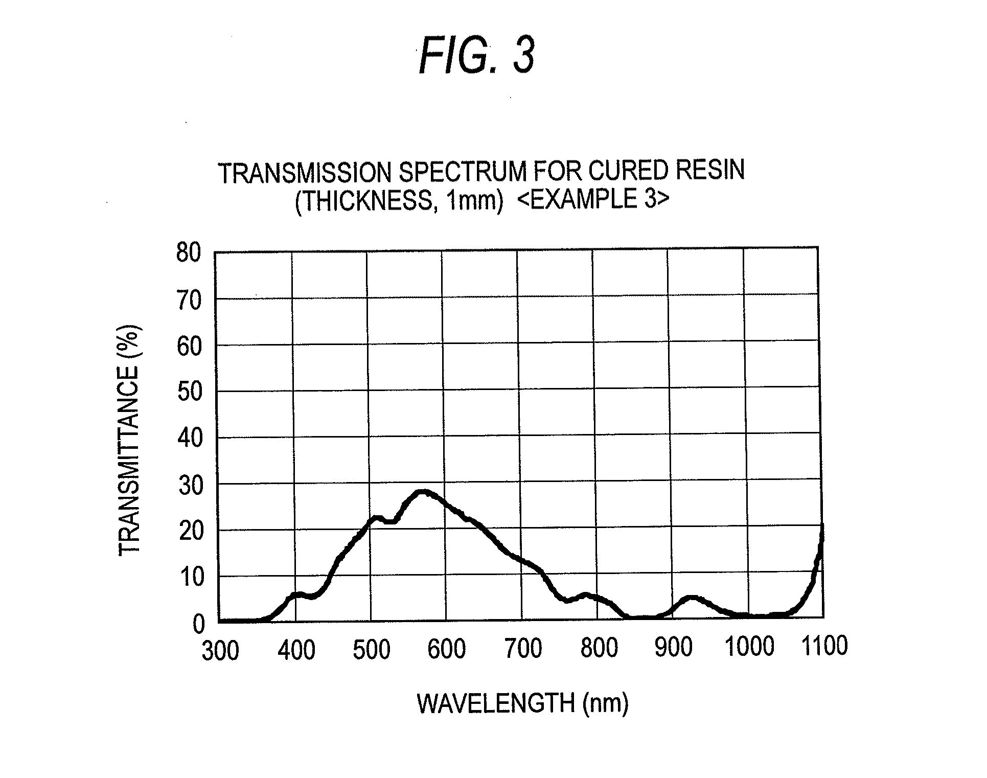
examples 1 to 3
[0078] A phthalocyanine colorant and naphthalocyanine colorants were added in the amounts shown in Table 1 below to a mixture composed of 100 parts of an epoxy resin, 99 parts of a curing agent, and 1 part of a curing accelerator as shown in the table.
[0079] Each liquid resin composition obtained (epoxy resin composition for optical-semiconductor encapsulation) was poured into a mold having a thickness of 1 mm and heated at 150° C. for 3 hours to obtain a cured resin composition. This cured resin composition (1-mm thick) was examined with apparatus UV-3101PC (manufactured by Shimadzu Corp.) for a transmission spectrum. The results obtained are shown in FIG. 1 (Example 1), FIG. 2 (Example 2), and FIG. 3 (Example 3). As apparent from FIGS. 1 to 3, the cured resins obtained in Examples 1 to 3 had a transmittance in the near infrared region (750 to 900 nm) of 5% or lower.
PUM
| Property | Measurement | Unit |
|---|---|---|
| wavelength range | aaaaa | aaaaa |
| wavelengths | aaaaa | aaaaa |
| wavelengths | aaaaa | aaaaa |
Abstract
Description
Claims
Application Information