Color display device and method for manufacturing the same

a color display and color filter technology, applied in the direction of discharge tube luminescnet screens, discharge tube/lamp details, electric discharge lamps, etc., can solve the problems of low luminous efficiency of white color filter material itself, difficulty in realizing high-definition or large-sized displays, and reduced luminance by color filters to about 13

Active Publication Date: 2010-03-04
UDC IRELAND
View PDF3 Cites 109 Cited by
  • Summary
  • Abstract
  • Description
  • Claims
  • Application Information

AI Technical Summary

Problems solved by technology

However, the separate forming technique is difficult so that realization of high-definition or large-sized displays is regarded as difficult.
In the method of combining color filters with a white organic EL device to attain the three colors, there is a problem that the luminous efficiency of a white color-emitting material itself is low, and the luminance is reduced by the color filters to about ⅓.
Various improvements have been made in a method of obtaining desired colors by converting the color of light from an organic EL device with a color conversion film, but there are problems such as low efficiency of conversion to red color, and the like.
This is because from the principle of a resonant that resonates light of specific wavelength only, arrangement of a resonant in the white sub-pixel region is not suitable for emitting white light having an emission spectrum in the whole visible range.
Accordingly, higher resolution is hardly attained, and the process is unfavorably complicated.

Method used


Image

  • Color display device and method for manufacturing the same
  • Color display device and method for manufacturing the same
  • Color display device and method for manufacturing the same

Examples


example 1

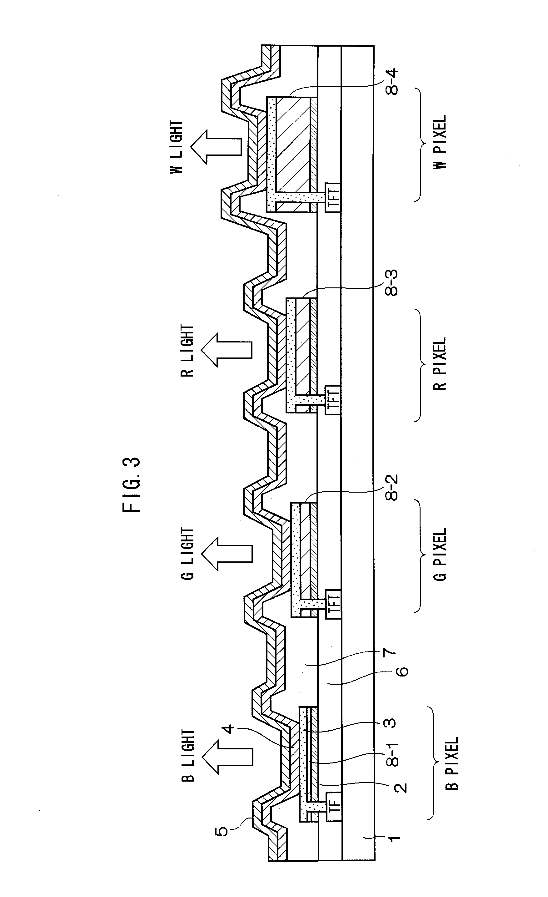
[0217]The method of manufacturing the color display device of the invention with the constitution shown in FIG. 3 is described.

[0218](1) On a glass substrate 1 provided with TFT, the TFT is covered with a planarizing film 6 of 3 μm in thickness. TFTs are arranged corresponding to R, G, B and W sub-pixels respectively.

[0219](2) On the planarizing film 6, Al is arranged to a thickness of 100 nm as a light reflection layer 2 by patterning in R, G, B and W sub-pixels respectively by the vacuum film-forming method.

[0220](3) On the upper surface of the light reflection layer 2, optical path length regulation layers 8-1, 8-2, 8-3 and 8-4 composed of a transparent insulating material which in the positions of R, G, B and W sub-pixels, is made different in film thickness.[0221]Material: SiON[0222]Film-forming method: ion plating method[0223]Thickness: 120 nm in R region, 70 nm in G region, 30 nm in B region, and 2200 nm in W region.

[0224](4) On the upper surface of the optical path length re...

example 2

[0241]The pixel in this example has the constitution shown in FIG. 4 which is the same as in Example 1 except that the constitution of the W sub-pixel region was changed as follows. The method of manufacturing each component is the same as in Example 1.

[0242](1) First, a light reflection layer 12-2 is arranged on a substrate 11 for a TFT.

[0243](2) The TFT and light reflection layer 12-2 are covered by arranging a planarizing film 16. The step of arranging the planarizing film 16 is carried out by the same step as in arranging the planarizing film 16 in the R, G and B sub-pixel regions.

[0244](3) The subsequent steps of laminating a transparent electrode 13 / white organic electroluminescence layer 14 / optically semitransparent reflection layer 15 are carried out by the same steps as in the R, G and B sub-pixel regions.

[0245]In the constitution obtained above, the planarizing film 16 in the W sub-pixel region functions as a substitute for the optical path length regulation layer. In this...

example 3

[0246]The pixel in this example has the constitution shown in FIG. 5 which is the same as in Example 2 except that even in the R, G and B sub-pixel regions, the light reflection layer is arranged in the planarizing film 26.

[0247](1) On substrate 21 for TFT, a light reflection layer 22-4 is first formed for W sub-pixel.

[0248](2) Throughout R, G, B and W sub-pixel regions, TFT and a light reflection layer 22-2 are covered by arranging a planarizing film of first thickness.

[0249](3) Then, a light reflection layer 22-3 is arranged for R sub-pixel.

[0250](4) Subsequently, a planarized plate of second thickness is arranged throughout the R, G, B and W sub-pixel regions.

[0251](5) Then, a light reflection layer 22-2 is arranged for G sub-pixel.

[0252](6) Subsequently, a planarizing film of third thickness is arranged throughout the R, G, B and W sub-pixel regions.

[0253](7) Then, a light reflection layer 22-1 is arranged for B sub-pixel.

[0254](8) Subsequently, a planarizing film of fourth thic...


PUM


Abstract

Disclosed is a color display device containing plural pixels on a substrate, each pixel is composed of plural sub-pixels which emit lights different in wavelength in the visible range and a white sub-pixel, the plural sub-pixels and the white sub-pixel each have a white organic electroluminescence layer interposed between an optically semitransparent reflection layer and a light reflection layer, the optical distance between the optically semitransparent reflection layer and the light reflection layer in each of the plural sub-pixels forms a resonator having a distance for resonating emitted light, and the optical distance between the optically semitransparent reflection layer and the light reflection layer in the white sub-pixel is longer than the maximum optical distance between the optically semitransparent reflection layer and the light reflection layer in each of the plural sub-pixels.

Description

CROSS-REFERENCE TO RELATED APPLICATION[0001]This application claims priority under 35 USC 119 from Japanese Patent Application No. 2008-221881 filed on Aug. 29, 2008, the disclosure of which is incorporated by reference herein.BACKGROUND[0002]1. Field of the Invention[0003]The present invention relates to a color display device using an electroluminescent device and a method for manufacturing the same.[0004]2. Related Art[0005]In recent years, thin and lightweight flat panel displays have been substituted for cathode ray tubes (CRTs) in various fields, and their applications are expanding. This is because personal information terminals such as personal computers and network access-compatible cell phones are acceleratingly spreading due to development of information equipments and infrastructures for services network with internet as a core. Further, the market of flat panel displays is expanding to household-use televisions that have conventionally been in the exclusive province of ...

Claims


Application Information

Patent Timeline
Patent Type & Authority Applications(United States)
IPC IPC(8): H01J1/54H01L21/77
CPCH01L51/5265H01L27/3213H10K59/351H10K50/852
Inventor KINOSHITA, MASARU
Owner UDC IRELAND
Why Eureka
Try Eureka