Spacer and electron emission display having the same

Inactive Publication Date: 2010-03-11
SAMSUNG SDI CO LTD
View PDF19 Cites 0 Cited by
  • Summary
  • Abstract
  • Description
  • Claims
  • Application Information

AI Technical Summary

Benefits of technology

[0014]It is another object of the present invention to provide a spacer that can suppress an electron beam distor

Problems solved by technology

The electron beam-diffusing phenomenon cannot be completely suppressed even when a focusing electrode is provided.
In this case, the space

Method used


Image

  • Spacer and electron emission display having the same
  • Spacer and electron emission display having the same
  • Spacer and electron emission display having the same

Examples


Embodiment Construction

[0029]The present invention will now be described more fully with reference to the accompanying drawings, in which exemplary embodiments of the invention are shown. The invention may, however, be embodied in many different forms and should not be construed as being limited to the embodiments set forth herein; rather these embodiments are provided so that this disclosure will be thorough and complete, and will fully convey the concept of the invention to those skilled in the art.

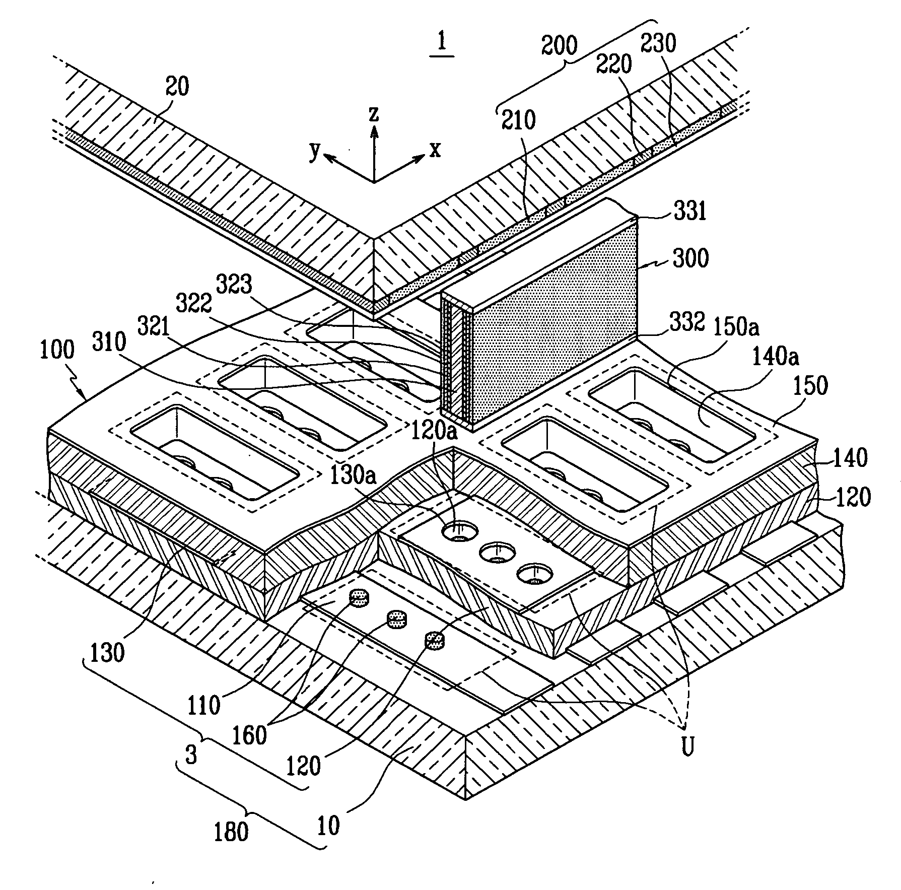
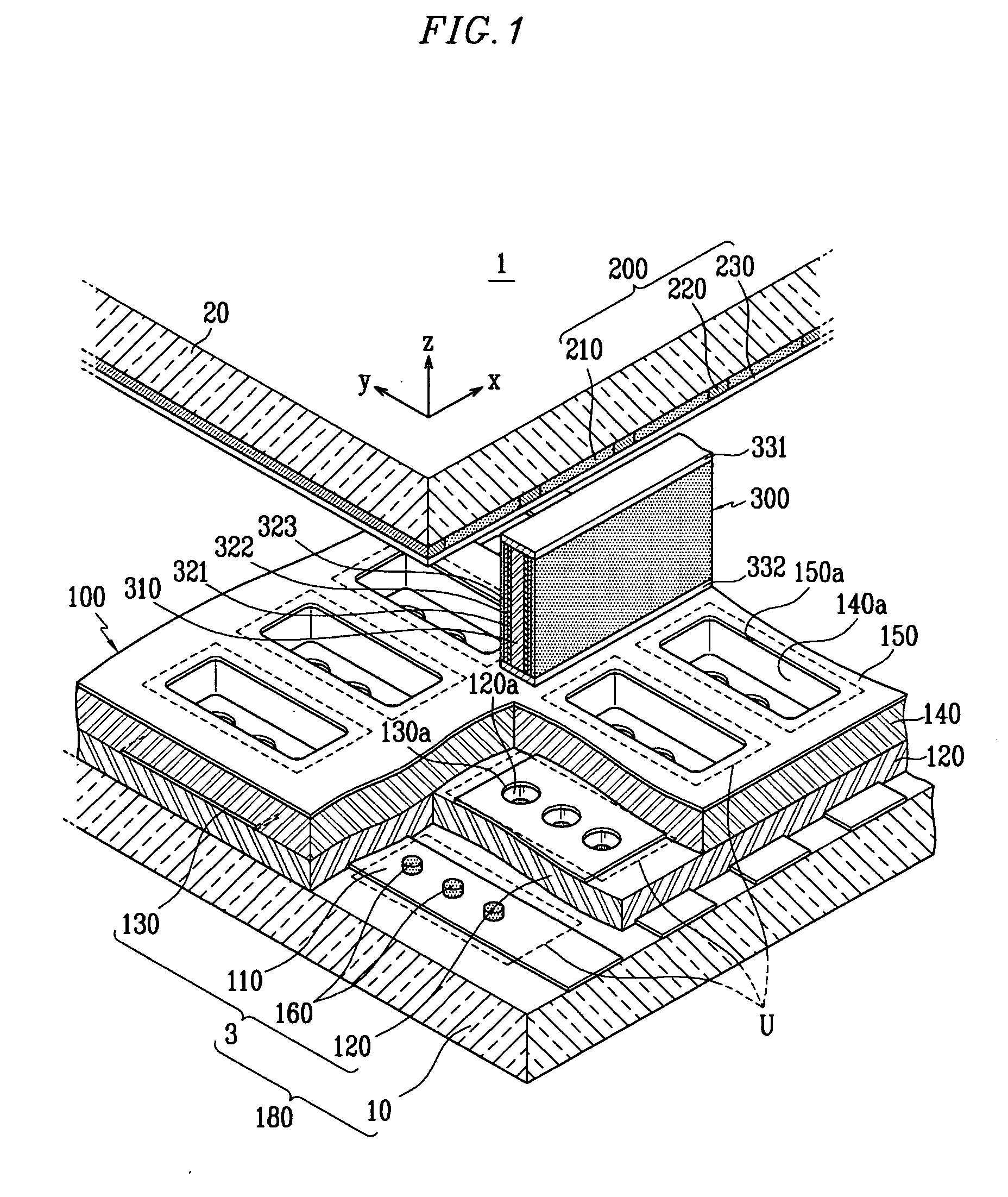
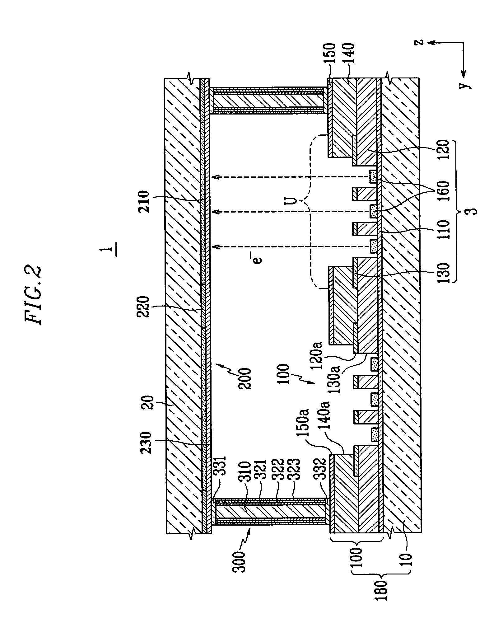
[0030]FIGS. 1 and 2 show an electron emission display constructed as an embodiment according to the principles of the present invention. In this embodiment, an electron emission display having an array of field emitter array (FEA) elements is illustrated.

[0031]Referring to FIGS. 1 and 2, an electron emission display 1 is constructed with first and second substrates 10 and 20 facing each other at a interval. A sealing member (not shown) is provided around the peripheries of first and second substrates 10 and 2...


PUM


Abstract

A spacer disposed between first and second substrates of an electron emission display is provided. The spacer includes a main body and a heat dissipation layer formed on a side surface of the main body.

Description

CLAIM OF PRIORITY[0001]This application makes reference to, incorporates the same herein, and claims all benefits accruing under 35 U.S.C. §119 from an application for SPACER AND ELECTRON EMISSION DISPLAY HAVING THE SAME earlier filed in the Korean Intellectual Property Office on 31 Oct. 2005 and there duly assigned Serial No. 10-2005-0103527.BACKGROUND OF THE INVENTION[0002]1. Field of the Invention[0003]The present invention relates to a spacer and an electron emission display incorporating the spacer, and more particularly, to a spacer that is designed to prevent electric charges from being accumulated on the surface of the spacer and an electron emission display incorporating the spacer.[0004]2. Description of the Related Art[0005]Generally, electron emission elements are classified as either those using hot cathodes as an electron emission source, or those using cold cathodes as the electron emission source. There are several types of cold cathode electron emission elements, in...

Claims


Application Information

Patent Timeline
IPC IPC(8): H01J61/52
CPCH01J29/864H01J2329/8645H01J2329/864H01J31/127
Inventor JIN, SUNG-HWANCHANG, CHEOL-HYEON
Owner SAMSUNG SDI CO LTD
Why Eureka
Try Eureka