Output buffer apparatus capable of adjusting output impedance in synchronization with data signal
Inactive Publication Date: 2005-12-27
RENESAS ELECTRONICS CORP
View PDF7 Cites 0 Cited by
Summary
Abstract
Description
Claims
Application Information
AI Technical Summary
This helps you quickly interpret patents by identifying the three key elements:
Problems solved by technology
Method used
Benefits of technology
Benefits of technology
[0011]It is an object of the present invention to provide an output buffer apparatus capable of suppressing the distortion of the output signal.
Problems solved by technology
Therefore, when reflection noise is generated at the terminal of the transmission line due to a discrepancy between the output impedance of the output buffer apparatus and the characteristic impedance of the transmission line, since the reflection noise may affect the transmitted signals, the transmitted signals are remarkably distorted.
In the above-described prior art output buffer apparatus, however, since the impedance adjusting signals are supplied to the pre-buffer circuit in asynchronization with the data signal, the output signal at the output terminal may be changed in the middle of data “1” or “0”, i.e., the output signal at the output terminal is distorted, thus deteriorating the quality thereof.
Method used
Image
Click on the blue label to locate the original text in one second.
Reading with bidirectional positioning of images and text.
Examples
first embodiment
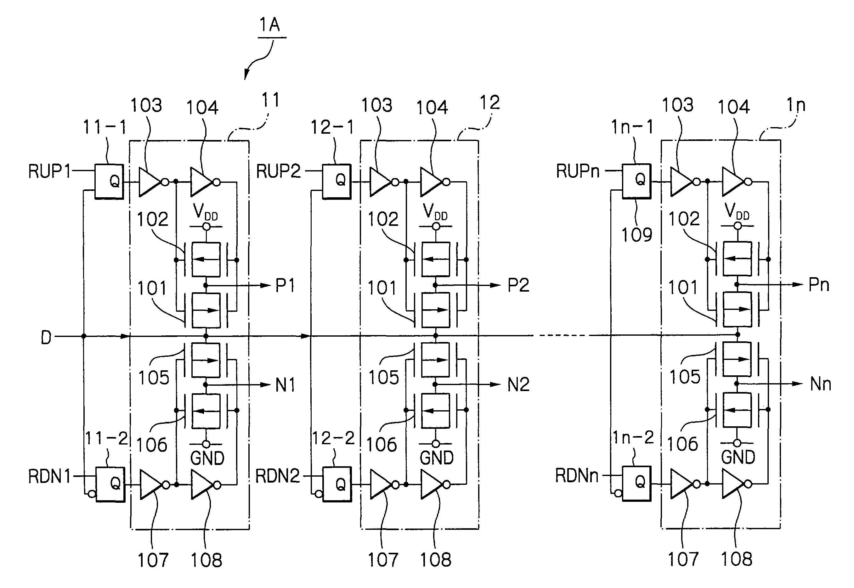
[0048]In FIG. 9, which illustrates the output buffer apparatus according to the present invention, the pre-buffer circuit 1 of FIG. 1 is replaced by a pre-buffer circuit 1A.
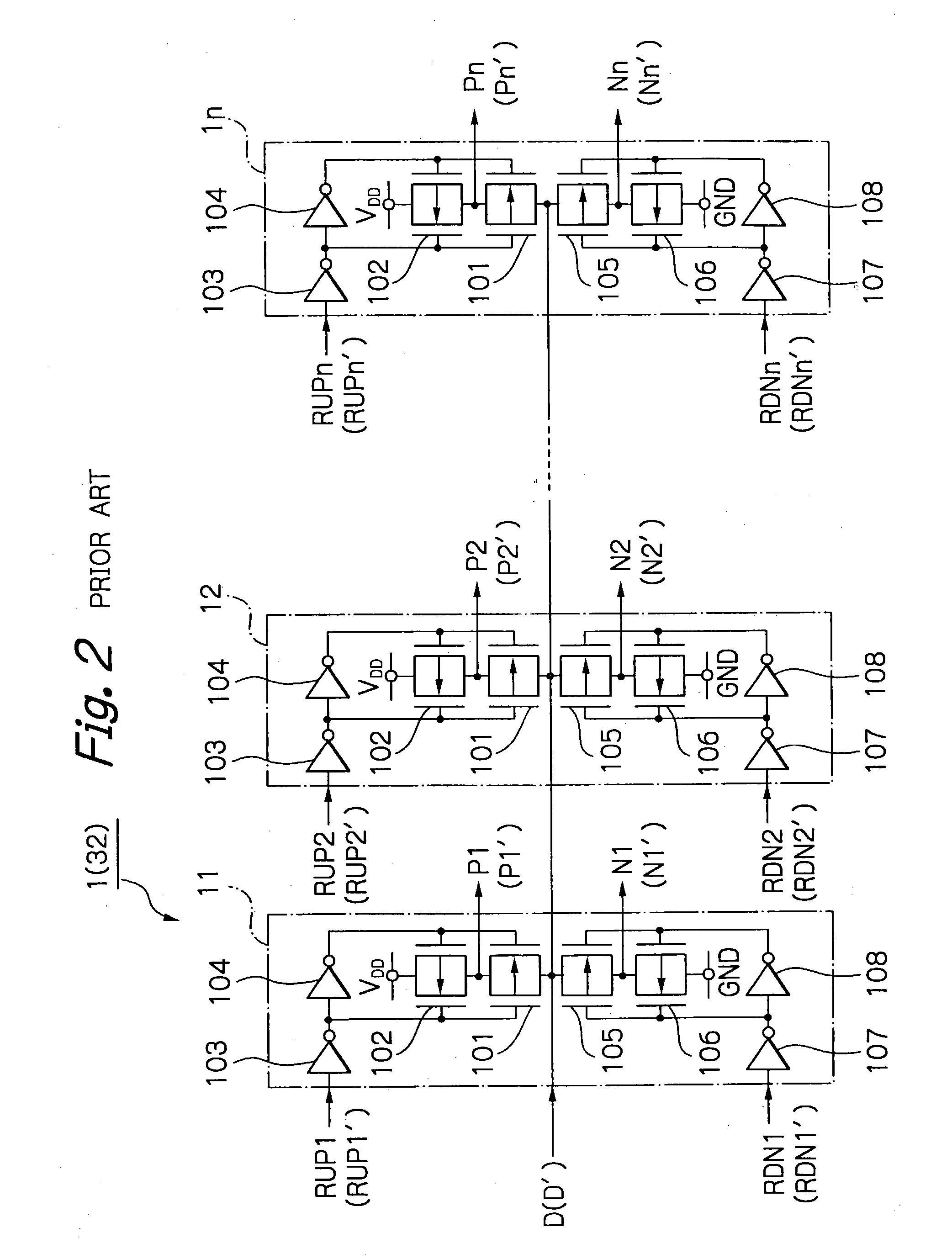
[0049]In FIG. 10, which is a detailed circuit diagram of the pre-buffer circuit 1A of FIG. 9, D-type flip-flops 11-1, 11-2, 12-1, 12-2, . . . , 1n-1, 1n-2 are added to the elements of the pre-buffer circuit 1 of FIG. 2.
[0050]The D-type flip-flop 1i-1 (i=1, 2, . . . , n) has a data input D for receiving the pull-up impedance adjusting signal RUPi, a clock terminal C for receiving the data signal D and an output terminal Q for generating an output signal which is transmitted to the inverter 103 of the pre-driver 1i. That is, the pull-up impedance adjusting signal RUPi is fetched by the D-type flip-flop 1i-1 in synchronization with a falling edge of the data signal D.
[0051]The D-type flip-flop 1i-2 (i=1, 2, . . . , n) has a data input D for receiving the pull-down impedance adjusting signal RDNi, a clock terminal C ...
second embodiment
[0055]In FIG. 12, which illustrates the output buffer apparatus according to the present invention, the pre-buffer circuit 1A of FIG. 9 is replaced by a pre-buffer circuit 1B.
[0056]In FIG. 13, which is a detailed circuit diagram of the pre-buffer circuit 1B of FIG. 12, latch circuits 11′-1, 11′-2, 12′-1, 12′-2, . . . , 1n′-1, 1n′-2 are provided instead of the D-type flip-flops 11-1, 11-2, 12-1, 12-2, . . . , 1n-1, 1n-2, respectively, of FIG. 10.
[0057]The latch circuit 1i′-1 (i=1, 2, . . . , n) is illustrated in detail in FIG. 14A. That is, the latch circuit 1i′-1 is constructed by inverters 1401 and 1402 for receiving the data signal D to generate clock signals C1 and its inverted signal, an inverter 1403 for receiving the pull-up impedance adjusting signal RUPi, a transfer gate 1404, inverters 1405 and 1406, a transfer gate 1407, and a buffer 1408 for generating a signal at an output terminal Q.
[0058]The operation of the latch circuit 1i′-1 (i=1, 2, . . . , n) is explained next wit...
PUM
Abstract
In an output buffer apparatus including a main-buffer circuit including a plurality of first transistors each connected between a first power supply terminal and an output terminal and a plurality of second transistors each connected between a second power supply terminal and the output terminal, and a pre-buffer circuit including a plurality of first pre-drivers each driving one of the first transistors in accordance with a data signal and a plurality of second pre-drivers each driving one of the second transistors in accordance with the data signal, a plurality of first sequential circuits are provided for receiving first impedance adjusting signals in synchronization with the data signal to turn ON the first pre-drivers, and a plurality of second sequential circuits are provided for receiving second impedance adjusting signals in synchronization with the data signal to turn ON the second pre-drivers.
Description
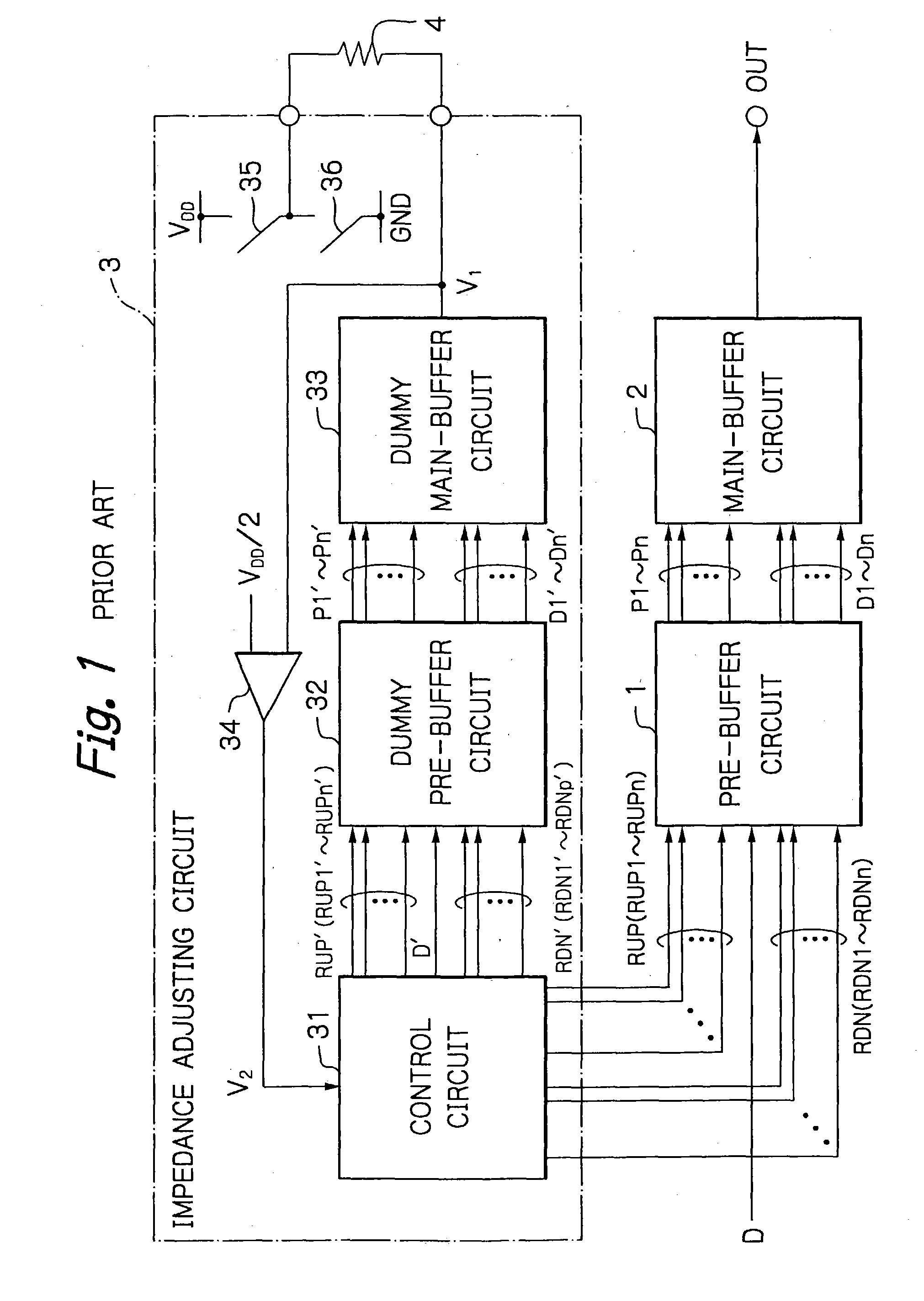
BACKGROUND OF THE INVENTION[0001]1. Field of the Invention[0002]The present invention relates to an output buffer apparatus capable of adjusting the output impedance thereof.[0003]2. Description of the Related Art[0004]In a computer system, as the speed of a central processing unit (CPU) has increased, the propagation speed of signals between semiconductor devices and the propagation speed of signals between printed circuit boards have also increased. Note that microstrip lines or coaxial cables are used as transmission lines for transmitting high frequency signals.[0005]When the frequency of transmitted signals is low, the wavelength of the transmitted signals is relatively large with respect to the length of the transmission line, so that the phases of the transmitted signals are approximately the same within the transmission line. Therefore, even when reflection noise is generated at a terminal of the transmission line due to a discrepancy between the output impedance of an outpu...
Claims
Application Information
Patent Timeline
Application Date:The date an application was filed.
Publication Date:The date a patent or application was officially published.
First Publication Date:The earliest publication date of a patent with the same application number.
Issue Date:Publication date of the patent grant document.
PCT Entry Date:The Entry date of PCT National Phase.
Estimated Expiry Date:The statutory expiry date of a patent right according to the Patent Law, and it is the longest term of protection that the patent right can achieve without the termination of the patent right due to other reasons(Term extension factor has been taken into account ).
Invalid Date:Actual expiry date is based on effective date or publication date of legal transaction data of invalid patent.

