Nonvolatile Memory Device and Method of Manufacturing the same
- Summary
- Abstract
- Description
- Claims
- Application Information
AI Technical Summary
Benefits of technology
Problems solved by technology
Method used
Image
Examples
first embodiment
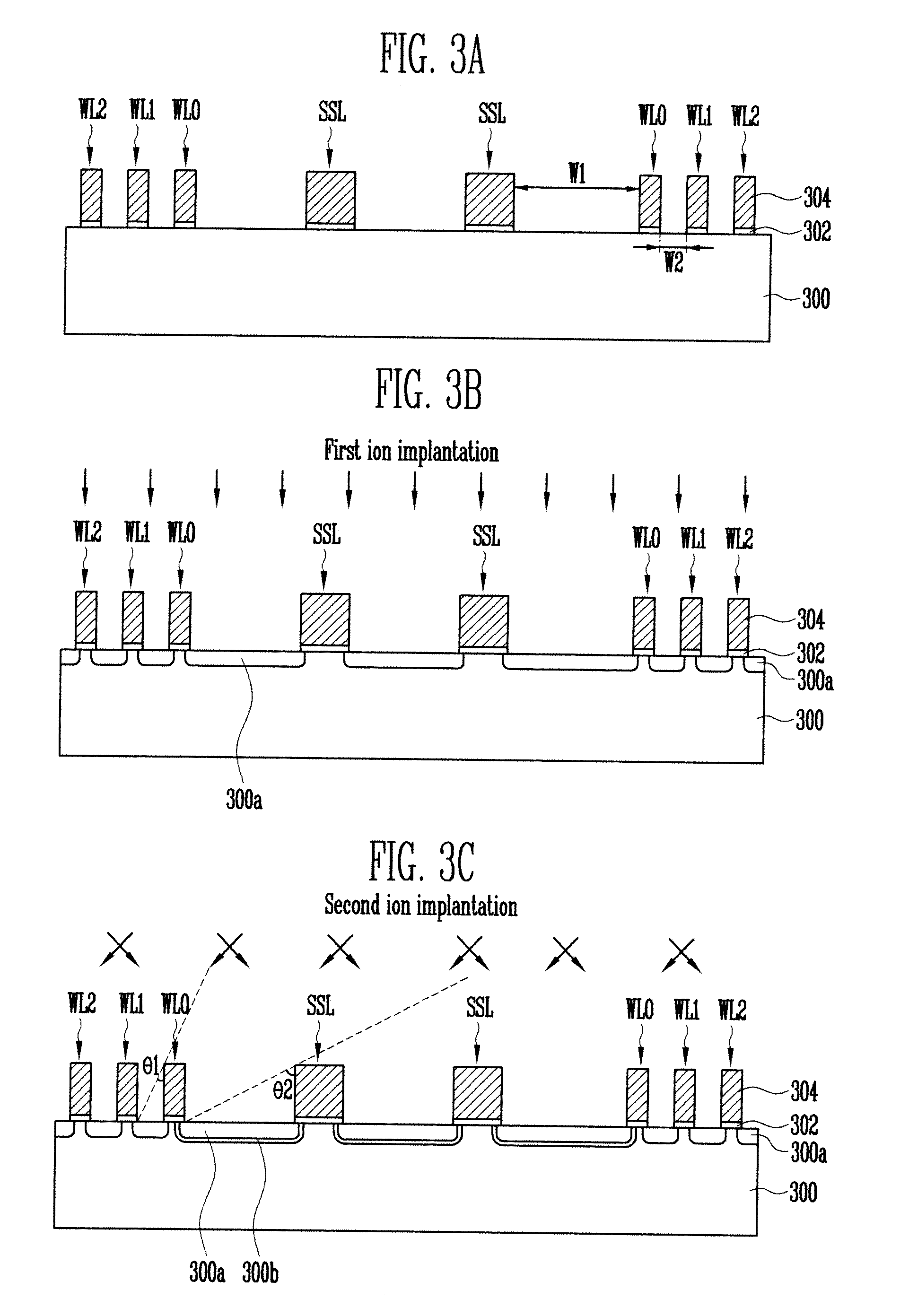
[0060]FIGS. 3A to 3C are sectional views illustrating a method of forming the junction regions of a nonvolatile memory device according to a
[0061]Referring to FIG. 3A, there is provided a semiconductor substrate 300 in which a well is formed. The well may be of an N-type or a P-type. A case where a P-type well is formed is described as an example. Gate lines 304 are formed over the semiconductor substrate 300 having the P-type well formed therein. The gate lines 304 include source select lines SSL and first to third word lines WL0 to WL2. Each of the source select lines SSL has a basic structure in which a gate insulation layer 302 and a gate are stacked. Each of the first to third word lines WL0 to WL2 has a basic structure in which the gate insulation layer 302, a floating gate, a dielectric layer, and a control gate are stacked. Since the source select line SSL transfers voltage higher than that of the first to third word lines WL0 to WL2, a first width W1 between the source sele...
second embodiment
[0068]FIG. 4 is a sectional view illustrating a method of forming the junction regions of a nonvolatile memory device according to a
[0069]Referring to FIG. 4, according to the description of FIGS. 3A and 3B, the first to third word lines WL0 to WL2 and the source select lines SSL are formed on the semiconductor substrate 300, and the first junction regions 300a are formed in the semiconductor substrate 300 exposed between the gate lines 304. Next, to protect the first junction regions 300a formed between the first to third word lines WL0 to WL2, a mask pattern 306 is formed on the first to third word lines WL0 to WL2 and on the first junction regions 300a between the first to third word lines WL0 to WL2. That is, the mask pattern 306 is opened at portions where the second junction regions 300b will be formed. The mask pattern 306 may be formed of a hard mask layer, but preferably may be formed of a photoresist layer.
[0070]After the mask pattern 306 is formed, the second junction reg...
third embodiment
[0071]FIG. 5 is a sectional view illustrating a method of forming the junction regions of a nonvolatile memory device according to
[0072]According to the description of FIGS. 3A and 3B, the first to third word lines WL0 to WL2 and the source select lines SSL are formed on the semiconductor substrate 300, and the first junction regions 300a are formed in the semiconductor substrate 300 exposed between the gate lines 304.
[0073]A spacer 308 is formed on the sidewalls of the source select lines SSL and the first to third word lines WL0 to WL2. The spacer 308 may be formed of an oxide layer. Here, when an etch process of forming a pattern for the spacer 308 is performed, the spacer 308 between the first to third word lines WL0 to WL2 remains without being etched because the distance between the first to third word lines WL0 to WL2 is narrow. Accordingly, the first junction regions 300a between the first to third word lines WL0 to WL2 are not exposed.
[0074]Next, when a fourth ion implantat...
PUM
 Abstract
Description
Claims
Application Information


