

Method of forming semiconductor device
- Summary
- Abstract
- Description
- Claims
- Application Information
AI Technical Summary
Benefits of technology
Problems solved by technology
Method used
Image

Examples
Embodiment Construction
[0023]Hereinafter, a method for forming a semiconductor device according to the present invention will be described with reference to the accompanying drawings.
[0024]FIGS. 4A to 4D are cross-sectional views illustrating a method for forming a semiconductor device according to the present invention.
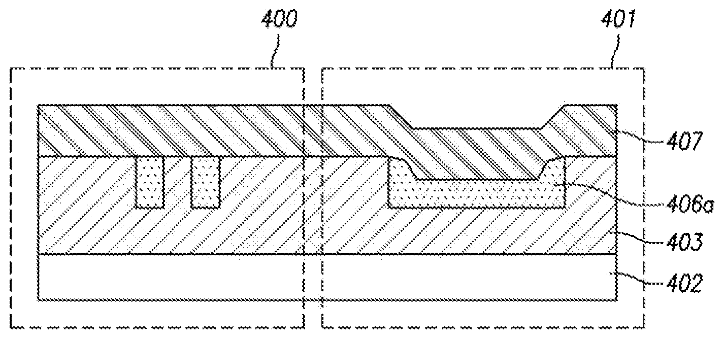
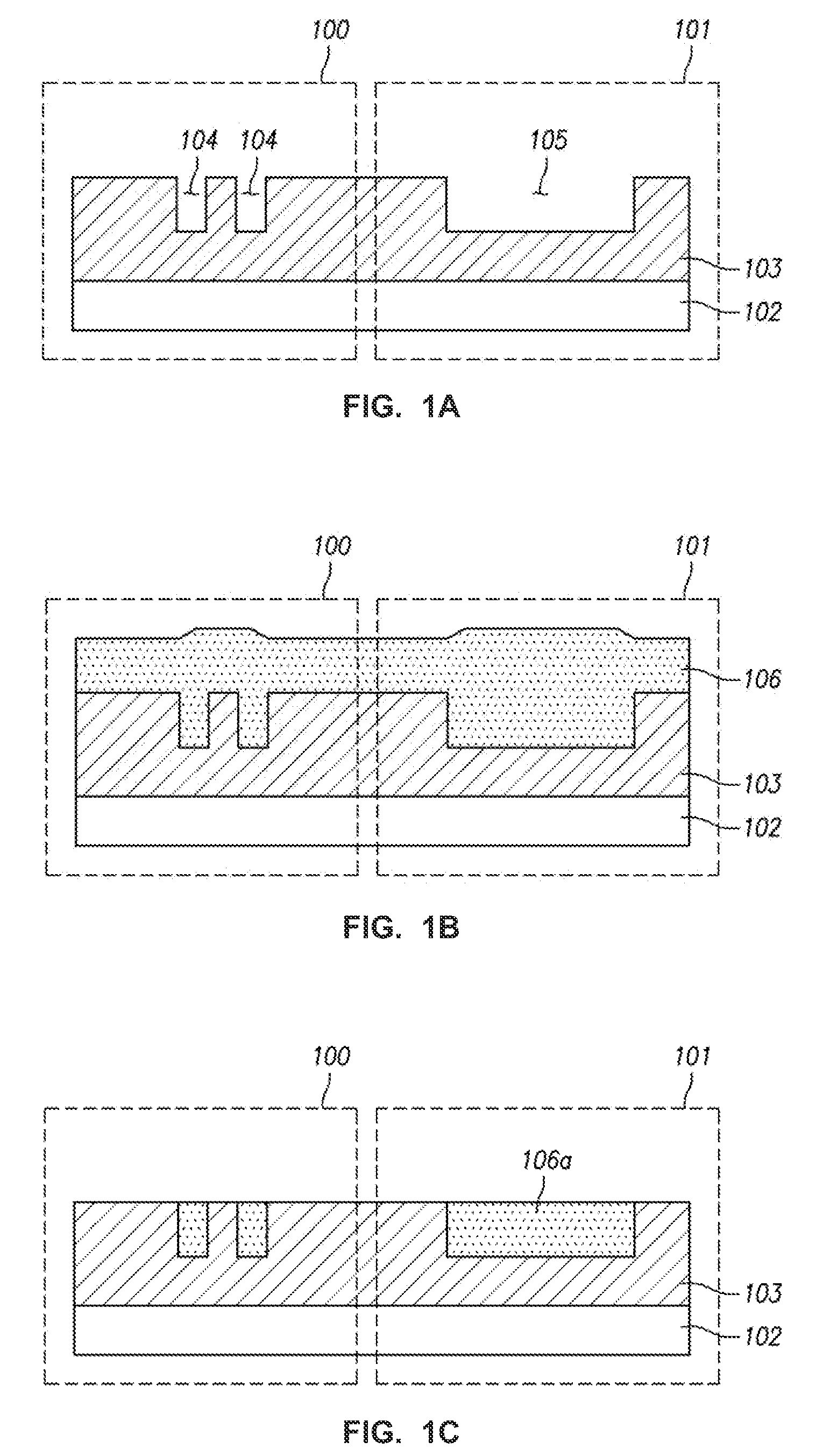
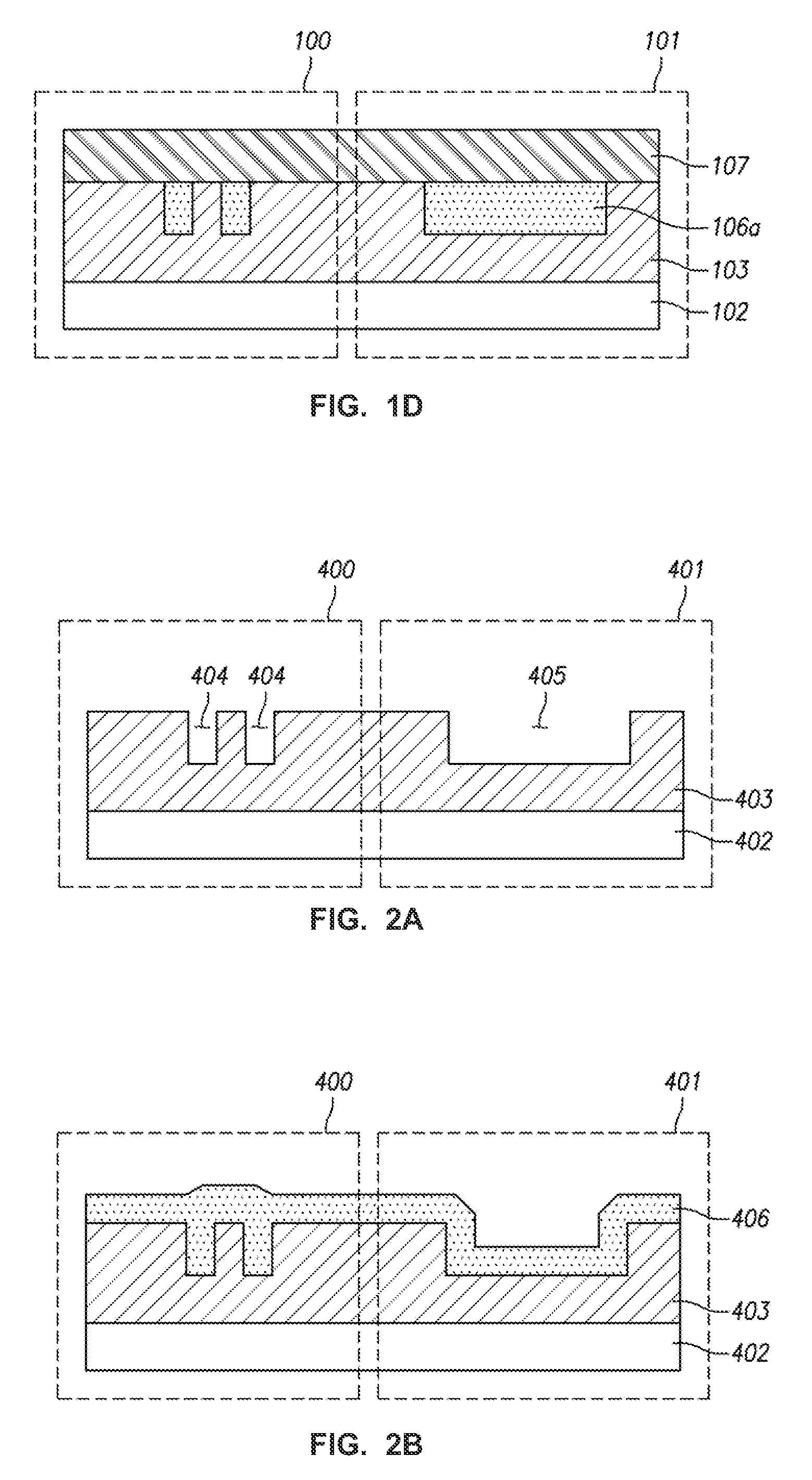
[0025]As shown in FIG. 4A, an inter-layer dielectric (ILD) layer 403 is formed on a semiconductor substrate 402 including a cell area 400 or a scribe lane area 401 so as to form at least one trench on the ILD layer 403. The trenches are formed by forming a photo resist pattern by coating a photoresist material and then forming it into a pattern.
[0026]Thereafter, an etching process is performed using the photo resist pattern as a mask so as to form a trench 405 in the scribe lane 401 with a width which is wider than the trench 404 of the cell area 400. Then ashing and cleaning processes are performed to remove the photo resist pattern.
[0027]Preferably, the trench 404 of the cell area 400 is...
PUM
 Abstract
Description
Claims
Application Information