Method for manufacturing a micro-electro-mechanical device with a folded substrate

a technology of micro-electromechanical devices and folded substrates, which is applied in the direction of microstructural devices, microstructure devices, microstructure technology, etc., can solve the problems of complex manufacturing process, inability to operate, damage to microstructure or semiconductor elements, etc., and achieve the effect of simplifying the forming process

Inactive Publication Date: 2010-08-03
SEMICON ENERGY LAB CO LTD
View PDF34 Cites 30 Cited by
  • Summary
  • Abstract
  • Description
  • Claims
  • Application Information

AI Technical Summary

Benefits of technology

[0014]In view of the foregoing, it is an object of the present invention to provide a micromachine (hereinafter referred to as a micro-electro-mechanical-device) having a microstructure and a semiconductor element over one surface. In particular, it is an object of the present invention to provide a method for simplifying the process of forming a microstructure and a semiconductor element over one surface.
[0027]As described above, in the present invention, the microstructure and the semiconductor element are formed over one surface. Conventionally, a space for moving the microstructure is formed by etching a sacrifice layer or deeply etching a silicon wafer. In the present invention however, a space is formed by processing an insulating layer which is formed in a manufacturing process of a semiconductor element. Therefore, a manufacturing process can be simplified, which leads to improvement in production efficiency and reduction in cost, and even reduction in damage of the microstructure being manufactured can be realized.
[0028]Thus, by manufacturing the microstructure and the semiconductor element over one surface, a micro-electro-mechanical device with simple assembly and package, and low manufacturing cost can be provided.

Problems solved by technology

However, when integrating a microstructure and a semiconductor element, the manufacturing process becomes complicated since the manufacturing process of the microstructure and that of the semiconductor element are different, e.g., etching of a sacrificial layer.
Since the processes are different, when integrating the microstructure and the semiconductor element, there is a possibility that the microstructure or the semiconductor element is damaged and does not operate.

Method used


Image

  • Method for manufacturing a micro-electro-mechanical device with a folded substrate
  • Method for manufacturing a micro-electro-mechanical device with a folded substrate
  • Method for manufacturing a micro-electro-mechanical device with a folded substrate

Examples


embodiments mode 1

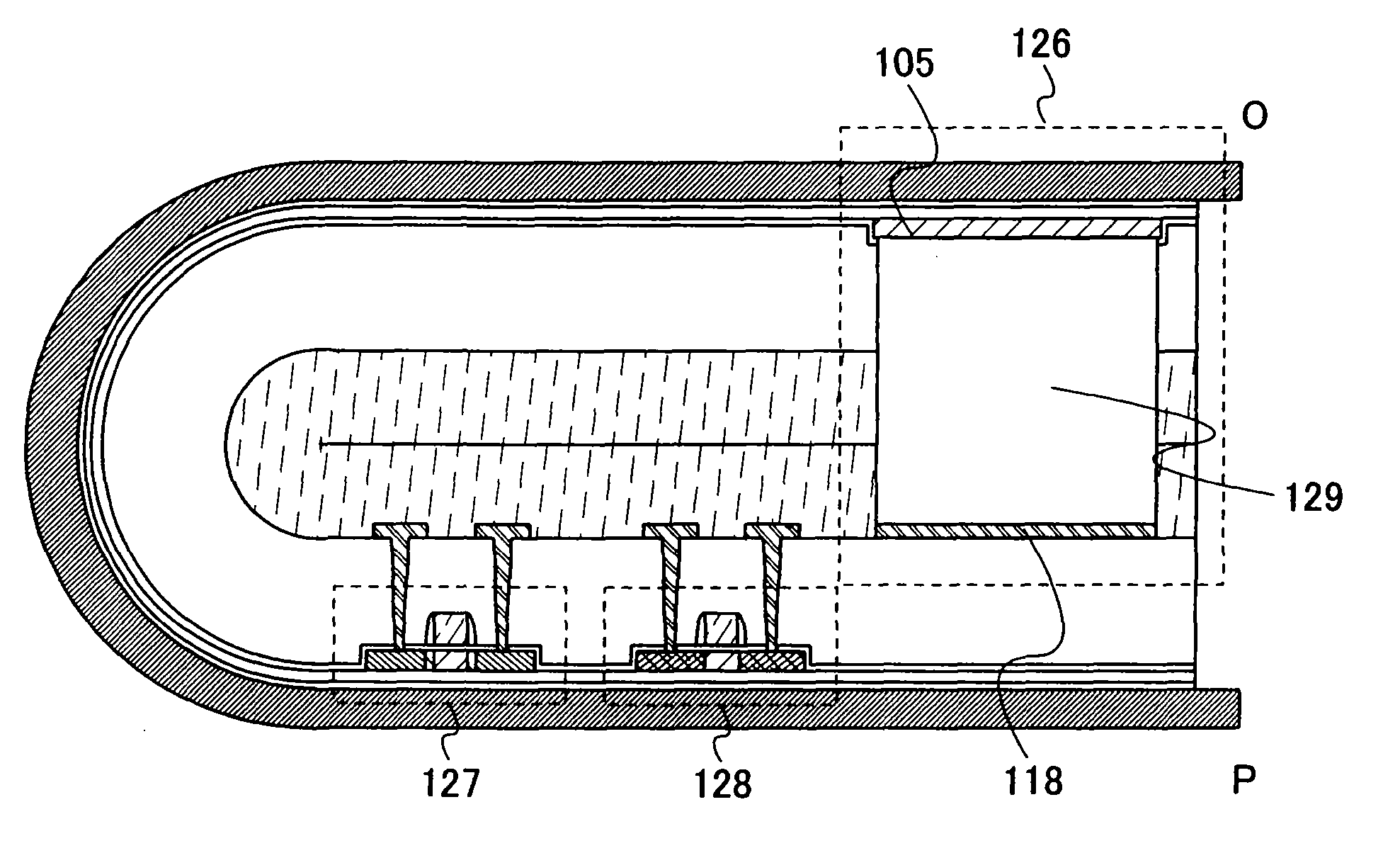
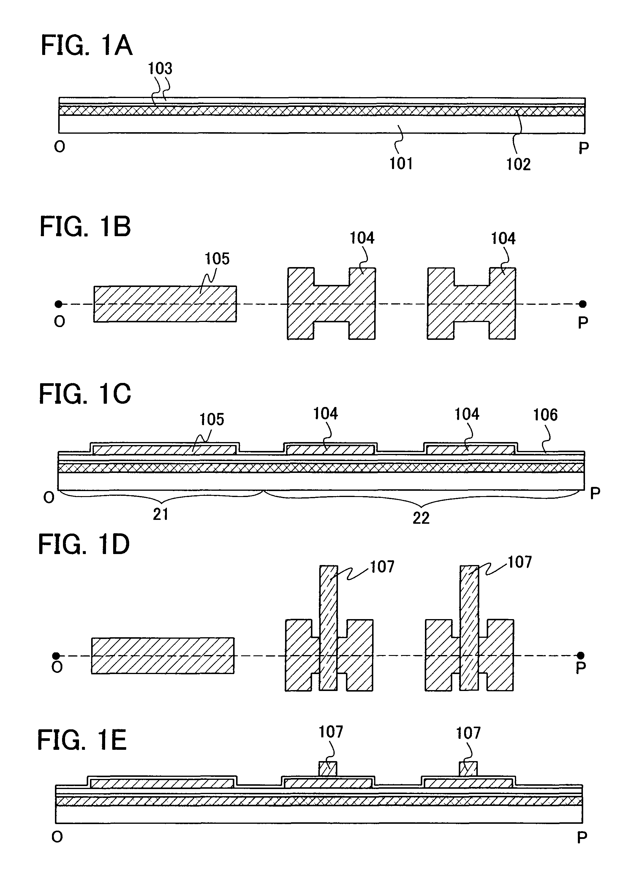
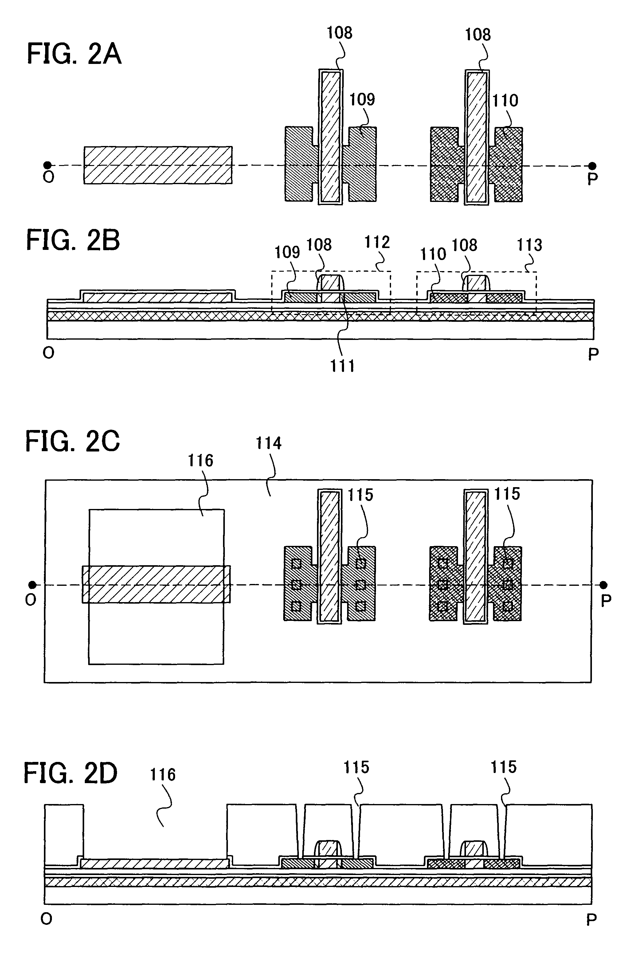
[0056]In this embodiment mode, a method of forming a microstructure and a semiconductor element over one surface is described with reference to the drawings. In the drawings, top views and cross-sectional views taken along a line O-P in the top views are shown.

[0057]A microstructure and a semiconductor element of the present invention can be formed over one surface of a substrate having an insulating property (insulating substrate). As an insulating substrate, there are a glass substrate, a quartz substrate, a plastic substrate, and the like. For example, by forming a microstructure and a semiconductor element over a plastic substrate, a light-weight micro-electro-mechanical device having high flexibility can be manufactured. In addition, by thinning a glass substrate by polishing or the like, a thin micro-electro-mechanical device can be manufactured. Further, a substrate obtained by forming a layer having an insulating property (insulating layer) over a conductive substrate such a...

embodiment mode 2

[0099]In this embodiment mode, a semiconductor layer having a crystalline structure, a microcrystalline structure, or an amorphous structure can be applied to the structure layer. In this embodiment mode, the case where polycrystalline silicon is used for the structure layer is described. Note that the structure layer may have a stacked-layer structure. When polycrystalline silicon is used for such a structure layer, polycrystalline silicon may be contained any of the layers. The structure layer can be also referred to as a layer containing polycrystalline silicon. Similarly, in the case of amorphous silicon, the structure layer can be also referred to as a layer containing amorphous silicon.

[0100]First, an amorphous silicon layer is formed over a surface for forming a structure layer. Then a thermal treatment is performed to crystallize the amorphous silicon layer, thereby a polycrystalline silicon layer can be obtained. A heating furnace, laser irradiation, irradiation with light ...

embodiment mode 3

[0121]In the present invention, silicon or silicon compounds having various properties can be stacked for the structure layer. Silicon layers having various properties are different in properties such as strength depending on the crystalline structure which is selected from an amorphous structure, microcrystalline structure, polycrystalline structure, or the like. Further, in the case of polycrystalline structure, a silicon layer thereof is different in properties due to the crystal direction. In this embodiment mode, an example of a stacked-layer structure used for the structure layer is described.

[0122]As shown in FIG. 6, silicon and silicon compounds which are different from each other in properties can be stacked. FIG. 6 shows the case where an amorphous silicon layer 150, a polycrystalline silicon layer 151, and a nickel silicide layer 152 are stacked as the structure layer 118 to form a space 153. Thus, by stacking layers different in mechanical properties, the structure layer...


PUM

PropertyMeasurementUnit
thicknessaaaaaaaaaa
thicknessaaaaaaaaaa
thicknessaaaaaaaaaa

Abstract

It is an object of the present invention to provide a micro-electro-mechanical-device having a microstructure and a semiconductor element over one surface. In particular, it is an object of the present invention to provide a method for simplifying the process of forming the microstructure and the semiconductor element over one surface. A space in which the microstructure is moved, that is, a movable space for the microstructure is formed by processing an insulating layer which is formed in a process of forming the semiconductor element. The movable space can be formed by forming the insulating layer having a plurality of openings and making the openings face each other to be overlapped each other.

Description

BACKGROUND OF THE INVENTION[0001]1. Field of the Invention[0002]The present invention relates to a micro-electro-mechanical device which has a microstructure and a semiconductor element, and a manufacturing method therefor.[0003]2. Description of the Related Art[0004]In recent years, a micro mechanical system called MEMS is actively researched. MEMS is an abbreviated name of a micro-electro-mechanical system, which is sometimes simply called a micromachine. A micromachine in general corresponds to a minute device in which “a movable microstructure having a three-dimensional structure” is integrated using a semiconductor minute processing technique. The microstructure has a three-dimensional structure, a movable portion, and a space for moving.[0005]A micromachine can control its microstructure by using an electronic circuit. Therefore, it is said that an autonomous decentralized type system can be formed which performs a series of operations by processing information obtained by a s...

Claims


Application Information

Patent Timeline
Patent Type & Authority Patents(United States)
IPC IPC(8): H01L21/00
CPCA61J3/00B81C1/0023C08F297/02H01L27/1266H01L27/1214Y02P20/582H01L27/1262H01L27/1218H01L27/1255B81C1/00B81B7/00
Inventor TATEISHI, FUMINORIIZUMI, KONAMIYAMAGUCHI, MAYUMI
Owner SEMICON ENERGY LAB CO LTD
Why Eureka
Try Eureka