Method for fabricating semiconductor memory device

Active Publication Date: 2005-04-21
PANNOVA SEMIC
View PDF10 Cites 0 Cited by
  • Summary
  • Abstract
  • Description
  • Claims
  • Application Information

AI Technical Summary

Benefits of technology

[0027] In the method of the present invention, the protective film is preferably a single layer of either a silicon nitride film or a silicon oxynitride film. Then, the process of forming the protective film is simplified.
[0028] In the method of the present invention, the protective film is preferably a multilayer film made of a plurality of insulating films including at least one of a silicon nitride film and a silicon oxynitride film. This method ensures protection of the isolation region and also ensures the use of the protective film as a trap film or an insulating film in the nonvolatile memory region.
[0029] In the method of the present invention, the multilayer film is preferably a stack of a silicon oxide film, either a silicon nitride film or a silicon oxynitride film, and a silicon oxide film. This method ensures protection of the isolation region and also ensures the use of the protective film as a trap film or an insulating film with more excellent function in the nonvolatile memory region. In addition, the staked films are easily etched in order.
[0030] In the method of the present invention, the step of introducing the impurity ions preferably includes a first impurity introducing step for forming a well and a second impurity introducing step for controlling a threshold volta

Problems solved by technology

If the logic circuit is optimized for the fabrication process for an embedded flash memory, desirable characteristics will not be obtained as well in a future process for fabricating a semiconductor device from which a nonvolatile memory has been removed.
However, the conventional method for fabricating a semiconductor memory device has the problem that the protective film, i.e., the ONO film, remaining on the isolation region causes charge to be captured in the protective film on the isolation region, so that the property of isolating the transistors deteriorates.
A silicon nitride film tends to capture charge, and thus charge is easily trapped in the silicon n

Method used


Image

  • Method for fabricating semiconductor memory device
  • Method for fabricating semiconductor memory device
  • Method for fabricating semiconductor memory device

Examples


Example

Embodiment 1

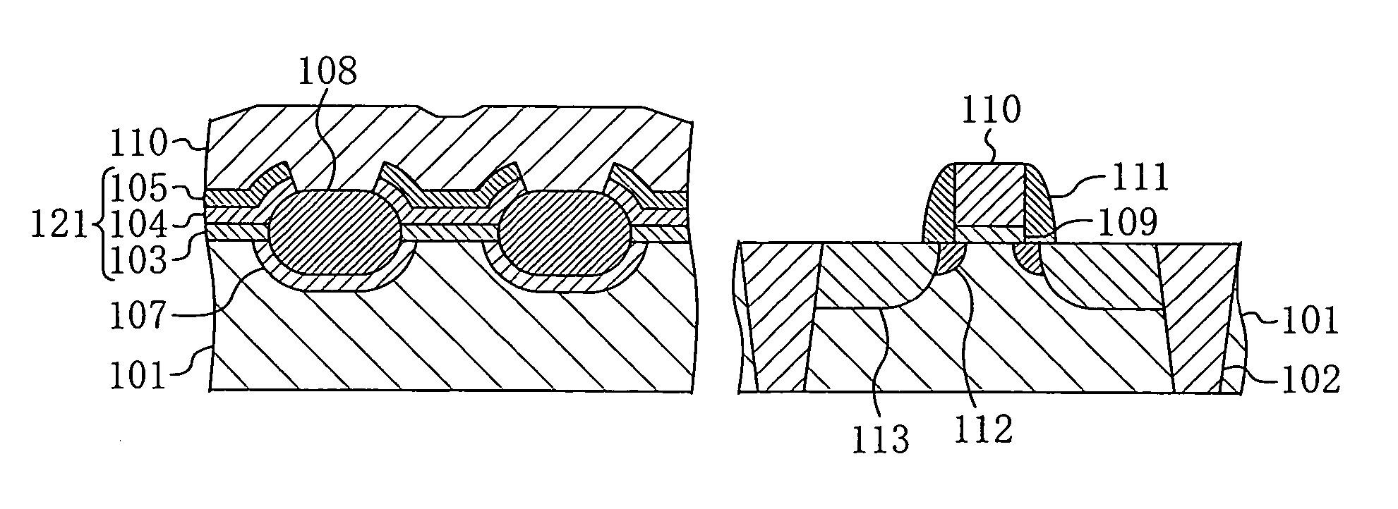
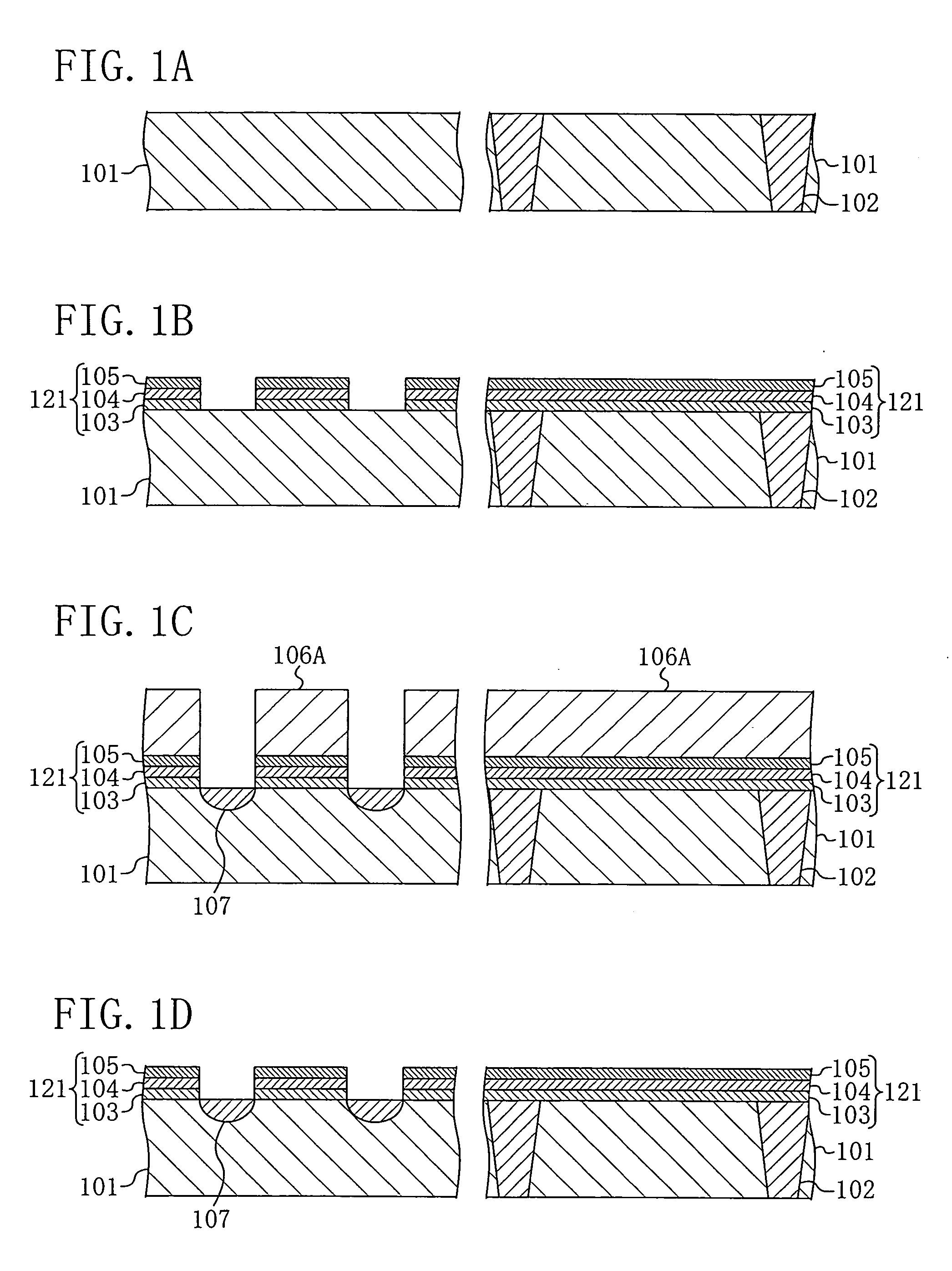
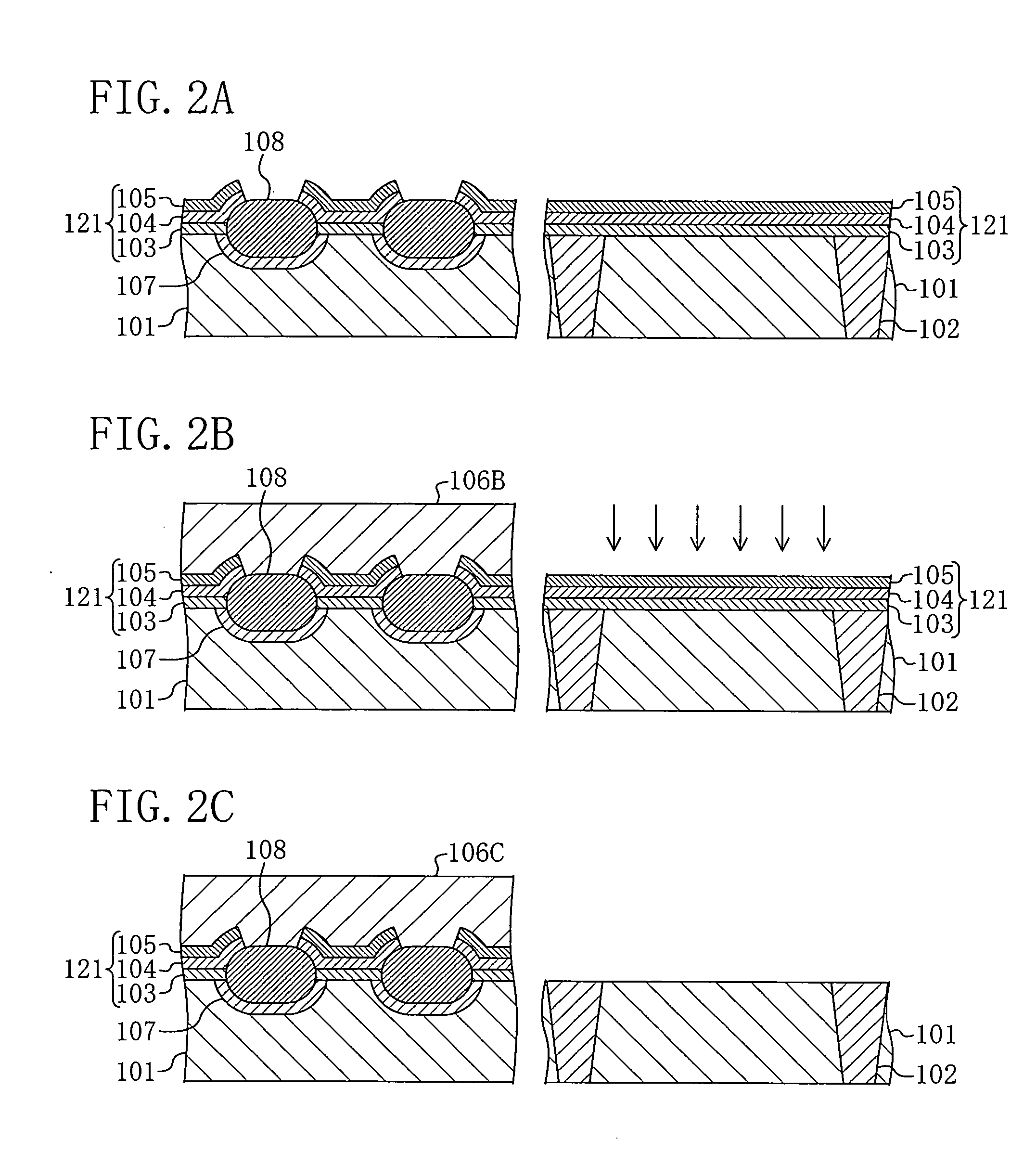
[0052]FIGS. 1A through 1D, 2A through 2C and 3A through 3D are cross-sectional views showing respective process steps of a method for fabricating a semiconductor memory device according to a first embodiment of the present invention. In FIGS. 1A through 3D, left-side parts represent a nonvolatile memory region (where a nonvolatile memory is to be formed) and right-side parts represent a logic circuit region (where a logic circuit is to be formed).

[0053] First, as shown in FIG. 1A, trenches whose sidewalls are vertical or tapered downward in cross section are formed in a semiconductor substrate 101 made of silicon in the logic circuit region. Then, a silicon oxide film is buried in the trenches, thereby forming isolation regions 102 serving as trench isolations.

[0054] Next, as shown in FIG. 1B, a lower oxide film 103 of silicon dioxide (SiO2) with a thickness of 7 nm, a silicon nitride film 104 of silicon nitride (SiN) with a thickness of 7 nm and an upper oxide film ...

Example

Embodiment 2

[0068]FIGS. 4A through 4D, 5A through 5E and 6A through 6D are cross-sectional views showing respective process steps of a method for fabricating a semiconductor memory device according to a second embodiment of the present invention. In FIGS. 4A through 6D, left-side parts represent a nonvolatile memory region and right-side parts represent a logic circuit region.

[0069] First, as shown in FIG. 4A, trenches whose sidewalls are vertical or tapered downward in cross section are formed in a semiconductor substrate 101 made of silicon in the logic circuit region. Then, a silicon oxide film is buried in the trenches, thereby forming isolation regions 102 serving as trench isolations.

[0070] Next, as shown in FIG. 4B, a lower oxide film 103 of silicon dioxide (SiO2) with a thickness of 7 nm, a silicon nitride film 104 of silicon nitride (SiN) with a thickness of 7 nm and an upper oxide film 105 of silicon dioxide (SiO2) with a thickness of 12 nm are formed in this order in b...

Example

Embodiment 3

[0086]FIGS. 7A through 7D, 8A, 8B, 9A, 9B, 10A through 10C and 11A through 11C are cross-sectional views showing respective process steps of a method for fabricating a semiconductor memory device according to a third embodiment of the present invention. In FIGS. 7A through 11C, left-side parts represent a nonvolatile memory region and right-side parts represent a logic circuit region.

[0087] First, as shown in FIG. 7A, trenches are formed in a semiconductor substrate 301 made of silicon in a nonvolatile memory region and a logic circuit region, and then trench isolation regions 302 are formed. Then, as shown in FIG. 7B, a tunnel insulating film 314 of SiO2 with a thickness of 10 nm is formed over the entire surface of the semiconductor substrate 301, and a polycrystalline silicon film 315 with a thickness of 200 nm to be a floating gate in the nonvolatile memory region is formed.

[0088] Next, as shown in FIG. 7C, the polycrystalline silicon film 315 and the tunnel insul...


PUM


Abstract

A method for fabricating a semiconductor memory device in which a logic circuit and a nonvolatile memory are provided on a semiconductor substrate includes the steps of: forming an isolation region; forming a protective film made of an insulating material over the semiconductor substrate in a logic circuit region and a nonvolatile memory region; selectively introducing impurity ions in part of the semiconductor substrate in the logic circuit region; and removing the protective film formed over the logic circuit region. The step of introducing the impurity ions is performed before the step of removing the protective film is performed.

Description

CROSS-REFERENCE TO RELATED APPLICATION [0001] The disclosure of Japanese Patent Application No. 2003-359641 filed in Oct. 20, 2003 including claims, specification and drawings is incorporated herein by reference in its entirety. BACKGROUND OF THE INVENTION [0002] The present invention relates to a method for fabricating a semiconductor device in which a logic circuit and a nonvolatile memory are incorporated. [0003] In recent years, to achieve multifunctionality and easy debugging, attention has been given to embedded flash memories in each of which a logic circuit and a nonvolatile memory are incorporated. A logic circuit incorporated in such an embedded flash memory needs to have the same function as that obtained when only the logic circuit is provided. [0004] To fabricate an embedded flash memory, however, a process for fabricating a nonvolatile memory needs to be added to a usual process for fabricating a logic circuit. This additional process for fabricating a nonvolatile memo...

Claims


Application Information

Patent Timeline
IPC IPC(8): H01L21/336H01L21/822H01L21/8234H01L21/8239H01L21/8246H01L21/8247H01L27/088H01L27/105H01L29/78
CPCH01L27/105H01L27/11526Y10S438/961H01L27/11568H01L27/11539H10B41/40H10B41/46H10B43/30
Inventor ARAI, MASATOSHI
Owner PANNOVA SEMIC
Why Eureka
Try Eureka