Nonvolatile Memory Device and Method of Manufacturing the Same

a nonvolatile memory and junction region technology, applied in the direction of semiconductor devices, electrical devices, transistors, etc., can solve the problems of large number of unit processes, complicated and inability to prevent the electrical properties of junction regions, so as to simplify the process of forming junction regions and prevent the effect of deterioration of electrical properties

Inactive Publication Date: 2012-03-15
SK HYNIX INC
View PDF1 Cites 0 Cited by
  • Summary
  • Abstract
  • Description
  • Claims
  • Application Information

AI Technical Summary

Benefits of technology

[0015]According to one or more embodiments, deterioration of the electrical properties of junction regions can be prohibited, and a process of forming the junction regions can be simplified.

Problems solved by technology

However, there is a limit to an increase of the distance between the source select line SSL and the adjacent first word line WL0 because of the degree of integration of nonvolatile memory devices.
Consequently, there is a problem in that a process of forming junction regions is complicated because the mask process must be repeatedly performed as many as the number of transistors including different junction regions.
Furthermore, to manufacture a nonvolatile memory device, a large number of unit processes must be performed.
Accordingly, a process of forming and removing ion implantation masks for selectively opening the junction regions must be performed several times. However, the process of forming and removing the ion implantation masks causes to increase the process expenses and the turn-around time.

Method used


Image

  • Nonvolatile Memory Device and Method of Manufacturing the Same
  • Nonvolatile Memory Device and Method of Manufacturing the Same
  • Nonvolatile Memory Device and Method of Manufacturing the Same

Examples


first embodiment

[0060]FIGS. 3A to 3C are sectional views illustrating a method of forming the junction regions of a nonvolatile memory device according to a

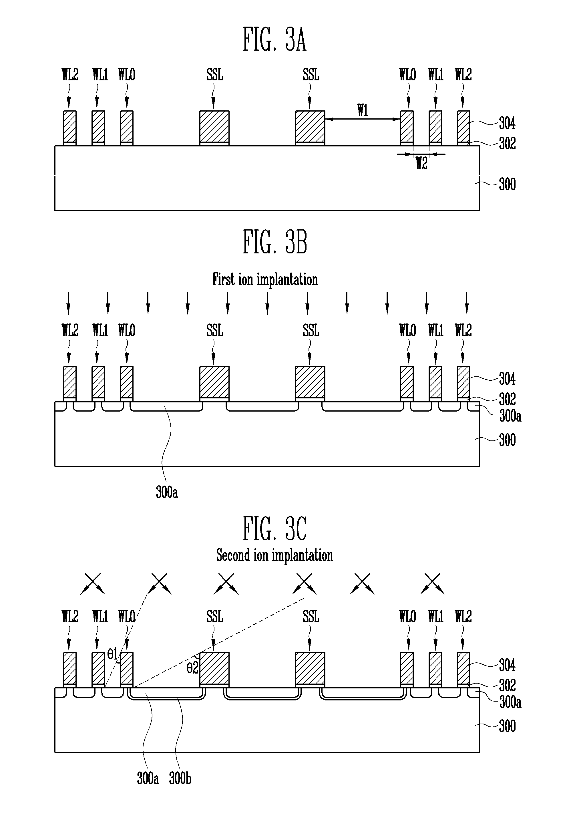
[0061]Referring to FIG. 3A, there is provided a semiconductor substrate 300 in which a well is formed. The well may be of an N-type or a P-type. A case where a P-type well is formed is described as an example. Gate lines 304 are formed over the semiconductor substrate 300 having the P-type well formed therein. The gate lines 304 include source select lines SSL and first to third word lines WL0 to WL2. Each of the source select lines SSL has a basic structure in which a gate insulation layer 302 and a gate are stacked. Each of the first to third word lines WL0 to WL2 has a basic structure in which the gate insulation layer 302, a floating gate, a dielectric layer, and a control gate are stacked. Since the source select line SSL transfers voltage higher than that of the first to third word lines WL0 to WL2, a first width W1 between the source sele...

second embodiment

[0068]FIG. 4 is a sectional view illustrating a method of forming the junction regions of a nonvolatile memory device according to a

[0069]Referring to FIG. 4, according to the description of FIGS. 3A and 3B, the first to third word lines WL0 to WL2 and the source select lines SSL are formed on the semiconductor substrate 300, and the first junction regions 300a are formed in the semiconductor substrate 300 exposed between the gate lines 304. Next, to protect the first junction regions 300a formed between the first to third word lines WL0 to WL2, a mask pattern 306 is formed on the first to third word lines WL0 to WL2 and on the first junction regions 300a between the first to third word lines WL0 to WL2. That is, the mask pattern 306 is opened at portions where the second junction regions 300b will be formed. The mask pattern 306 may be formed of a hard mask layer, but preferably may be formed of a photoresist layer.

[0070]After the mask pattern 306 is formed, the second junction reg...

third embodiment

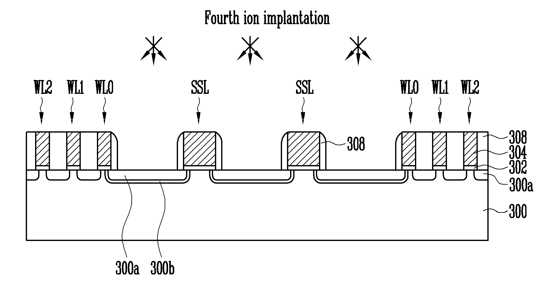
[0071]FIG. 5 is a sectional view illustrating a method of forming the junction regions of a nonvolatile memory device according to

[0072]According to the description of FIGS. 3A and 3B, the first to third word lines WL0 to WL2 and the source select lines SSL are formed on the semiconductor substrate 300, and the first junction regions 300a are formed in the semiconductor substrate 300 exposed between the gate lines 304.

[0073]A spacer 308 is formed on the sidewalls of the source select lines SSL and the first to third word lines WL0 to WL2. The spacer 308 may be formed of an oxide layer. Here, when an etch process of forming a pattern for the spacer 308 is performed, the spacer 308 between the first to third word lines WL0 to WL2 remains without being etched because the distance between the first to third word lines WL0 to WL2 is narrow. Accordingly, the first junction regions 300a between the first to third word lines WL0 to WL2 are not exposed.

[0074]Next, when a fourth ion implantat...


PUM


Abstract

A method of manufacturing a nonvolatile memory device wherein first gate lines and second gate lines are formed over a semiconductor substrate. The first gate lines are spaced-from each other at a first width, the second gate lines are spaced-from each other at a second width, and the first width is wider than the second width. A first ion implantation process of forming first junction regions in the semiconductor substrate between the first gate lines and the second gate lines is performed. A second ion implantation process of forming second junction regions in the respective first junction regions between the first gate lines is then performed.

Description

CROSS-REFERENCE TO RELATED APPLICATIONS[0001]This is a division of U.S. application Ser. No. 12 / 562,727 filed Sep. 18, 2009, which claims the priority benefit under USC 119 of KR 10-2008-0091987 filed Sep. 19, 2008, KR 10-2008-0133107 filed Dec. 24, 2008, and KR 10-2009-0045402 filed May 25, 2009, the entire respective disclosures of which are incorporated herein by reference.BACKGROUND[0002]Embodiments of the disclosure relate generally to a nonvolatile memory device and a method of manufacturing the same, and more particularly, to the junction regions of a nonvolatile memory device.[0003]In a nonvolatile memory device, memory cells for storing data are interconnected in series within the same string. The memory cells are electrically interconnected through junction regions within the same string.[0004]FIG. 1 is a sectional view of a known nonvolatile memory device.[0005]The nonvolatile memory device of FIG. 1 may be implanted by forming a number of gate lines on a semiconductor su...

Claims


Application Information

Patent Timeline
Patent Type & Authority Applications(United States)
IPC IPC(8): H01L27/088H01L21/8234
CPCH01L21/26586H01L27/11521H01L29/7833H01L29/6659H01L27/11529H10B41/41H10B41/30
Inventor LEE, HEE YOULNOH, JAE YOON
Owner SK HYNIX INC
Why Eureka
Try Eureka