Multi-layered device

a multi-layer device and multi-layer technology, applied in the direction of transformer/inductance details, printed inductances, basic electric elements, etc., can solve the problem of increasing the thickness of multi-layer devices, and achieve the effect of thinning the devi

Inactive Publication Date: 2010-04-01
MATSUSHITA ELECTRIC WORKS LTD
View PDF8 Cites 15 Cited by
  • Summary
  • Abstract
  • Description
  • Claims
  • Application Information

AI Technical Summary

Benefits of technology

[0010]According to such a configuration, since the first conductor which constitutes the first coil is formed on the first face of each foldable area and the second conductor which constitutes the second coil having the same winding direction as that of the first coil is formed on the second face, by folding the insulation sheet so that respective foldable areas are folded, at least four layers of the conductors constituting coils having the same winding directions are multilayered via the insulation sheets. Consequently, in comparison with the conventional multilayered device in which the conductors are formed on only one side of the insulation sheet, when a number of layers of the conductors of the devices are the same, it is possible to downsize and to thin the device. Alternatively, when the sizes of the devices are substantially the same, it is possible to obtain an inductor having a larger inductance value or a capacitor having a larger capacitance value.

Problems solved by technology

According to the above mentioned conventional multilayered device, since the coil shaped conductors are provided on only one face of the flexible insulation sheet 1 (SIC: 100), in order to constitute a coil device having a large number of turns, it is necessary to superimpose the single-sided flexible insulation sheets 1 (SIC: 100) each of which is folded to contact the rear faces several times via insulation sheets, and thus, there is a problem that a thickness of the multilayered device increases.

Method used


Image

  • Multi-layered device
  • Multi-layered device
  • Multi-layered device

Examples


first embodiment

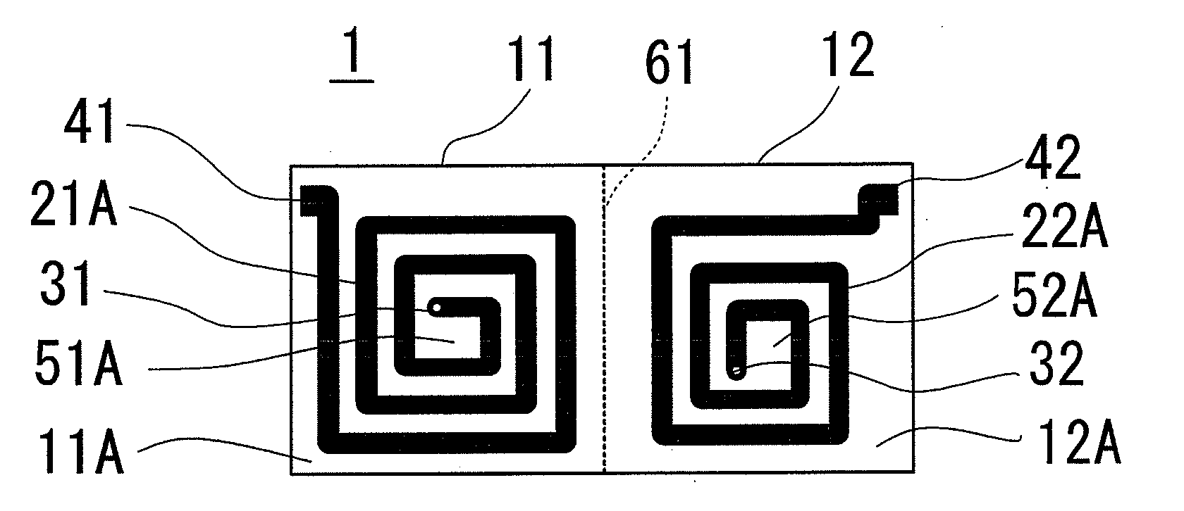
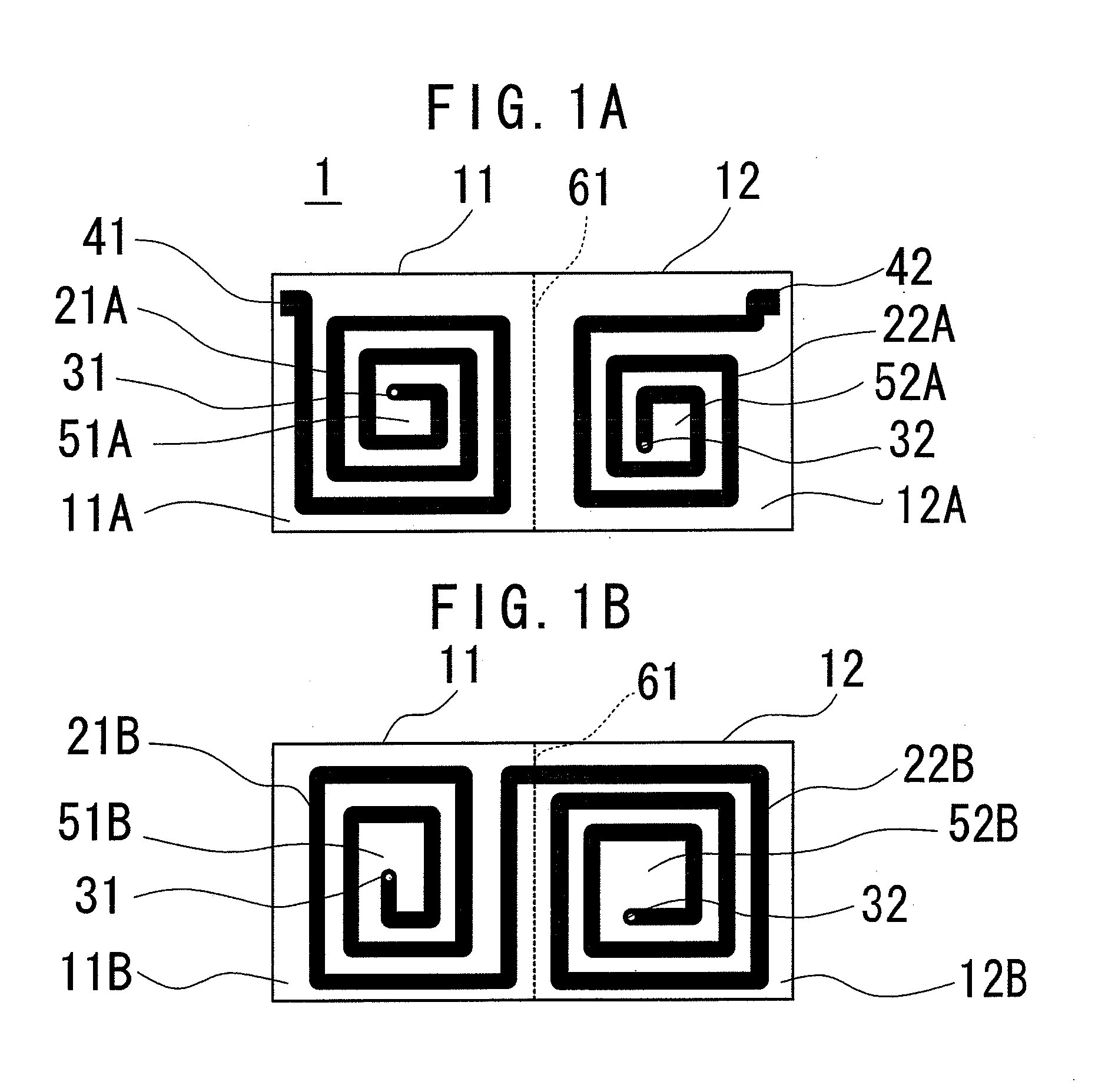
[0026]A multilayered device in accordance with a first embodiment of the present invention is described with reference to FIG. 1A and FIG. 1B. FIG. 1A shows a configuration of and patterns of conductors on a first face (front face) of an insulation sheet 1 which constitutes the multilayered device, and FIG. 1B shows a configuration of and patterns of conductors on a second face (rear face) thereof. Hereupon, the patterns of the conductors on the second face (rear face) shown in FIG. 1B are illustrated as patterns transparently observed from the same side of the patterns of the first face (front face). Therefore, when the patterns of the conductors on the second face (rear face) are observed from the second face side, the delineation will be reversed (the same goes for the following embodiments).

[0027]As shown in FIG. 1A and FIG. 1B, in the multilayered device in accordance with the first embodiment, the insulation sheet 1 has two foldable areas, that is, the first foldable area 11 a...

second embodiment

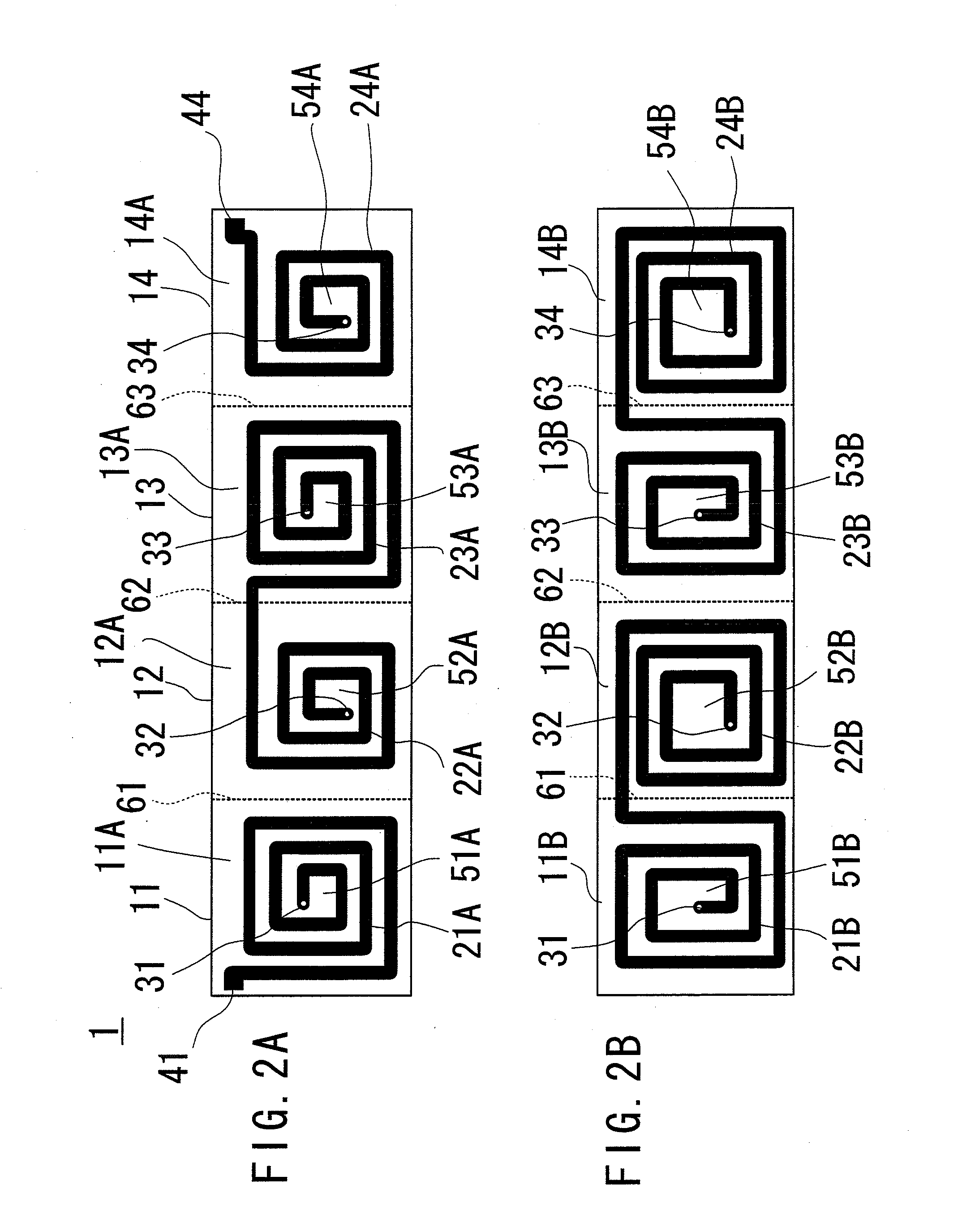
[0032]Subsequently, a multilayered device in accordance with a second embodiment of the present invention is described with reference to FIG. 2A and FIG. 2B. FIG. 2A shows a configuration of and patterns of conductors on a first face (front face) of an insulation sheet 1 which constitutes the multilayered device, and FIG. 2B shows a configuration of and patterns of conductors on a second face (rear face) thereof. Hereupon, the patterns of the conductors on the rear face shown in FIG. 2B are illustrated as patterns transparently observed from the same side of the patterns of the front face, similar to the above mentioned first embodiment. In addition, explanation of elements common in the above mentioned first embodiment are omitted (the same goes for the following embodiments).

[0033]In the second embodiment shown in FIG. 2A and FIG. 2B, an insulation sheet 1 is configured by four foldable areas 11 to 14. With respect to two foldable areas 11 and 12 adjoining each other, a foldable a...

third embodiment

[0037]Subsequently, a multilayered device in accordance with a third embodiment of the present invention is described with reference to FIG. 3A and FIG. 3B. FIG. 3A shows a configuration of and patterns of conductors on a first face (front face) of an insulation sheet 1 which constitutes the multilayered device, and FIG. 3B shows a configuration of and patterns of conductors on a second face (rear face) thereof. Hereupon, the patterns of the conductors on the rear face shown in FIG. 3B are illustrated as patterns transparently observed from the same side of the patterns of the front face, similar to the above mentioned first embodiment.

[0038]The multilayered device in accordance with the third embodiment is configured as a transformer having two windings. An insulation sheet 1 has two foldable areas, that is, a first foldable area 11 and a second foldable area 12, which are to be multilayered by being folded. First conductors 21A and 22A, which constitute first coils 51A and 52A eac...


PUM

PropertyMeasurementUnit
areaaaaaaaaaaa
inductanceaaaaaaaaaa
foldable areaaaaaaaaaaa

Abstract

A multilayered device comprises an insulation sheet 1 having at least two foldable areas 11, 12 which are multilayered by being folded; and a first conductor 21A, 22A which is formed on a first face 11A, 12A and constitutes a first coil 51A, 52A having one turn or more, and a second conductor 21B, 22B which is formed on a second face 11B, 12B and constitutes a second coil 51B, 52B having one turn or more in the same winding direction as that of the first coil in each of the foldable areas, at least four conductors are disposed in parallel with each other by folding the insulation sheet so as to constitute an inductor, and thus, it enables to thin the thickness of the multilayer, to downsize and to lightweight even when it constitutes a coil device having a larger winding number.

Description

TECHNICAL FIELD[0001]The present invention relates to a multilayered device which is configured by laminating insulation sheets with conductor coils.BACKGROUND ART[0002]For example, Japanese Laid-Open Patent Publication No. 5-243057 discloses a conventional multilayered device (a thin transformer) which is configured by laminating insulation sheets with conductor coils. In such conventional multilayered device, as shown in FIG. 14, conductors 200 which are formed of a material such as copper foil of a flexible printed circuit board to have coil shapes on a first face (front face) of a flexible insulation sheet 100 of foldable such as the flexible printed circuit board, for example. By laminating such insulation sheet 100, a multilayered device having a desired inductance value can be obtained.[0003]FIG. 15A and FIG. 15B are figures respectively showing a first face (a front face) and a second face (a rear face) of adjoining two folded areas of the insulation sheet 100. In this examp...

Claims


Application Information

Patent Timeline
Patent Type & Authority Applications(United States)
IPC IPC(8): H01F5/00
CPCH01F17/0006H01F2027/2861H01F2027/2819H01F27/2804
Inventor OKAWA, MASANAOKONISHI, HIROFUMI
Owner MATSUSHITA ELECTRIC WORKS LTD
Why Eureka
Try Eureka