Touch location detecting panel having a simple layer structure

a layer structure and touch location technology, applied in the field of touch location detecting panels, can solve the problems of increasing the lamination thickness of the touch location detecting panel, the discrete location detecting method has a limited touch location detecting resolution, and the manufacturing cost of the detecting panel is increased accordingly. , to achieve the effect of low manufacturing cost and simple layer structur

Active Publication Date: 2010-04-15
MELFAS
View PDF19 Cites 112 Cited by
  • Summary
  • Abstract
  • Description
  • Claims
  • Application Information

AI Technical Summary

Benefits of technology

[0012]It is, therefore, an object of the present invention to provide a touch location detecting panel which has a simple layer structure and requires low manufacturing costs.

Problems solved by technology

Meanwhile, the discrete location detecting method has a limited touch location detecting resolution which is dependent on an arrangement pitch of sensing areas.
In this case, however, the lamination thickness of the touch location detecting panel increases, and manufacturing cost of the detecting panel is increased accordingly.
Unfortunately, however, the formation of the ITO pattern layers requires a costly process, and since the conventional touch location detecting panel has even two sensing layers 10 and 20 having such high manufacturing costs, total manufacturing cost is increased.

Method used


Image

  • Touch location detecting panel having a simple layer structure
  • Touch location detecting panel having a simple layer structure
  • Touch location detecting panel having a simple layer structure

Examples


Embodiment Construction

[0024]Hereinafter, a touch location detecting panel in accordance with the present invention will be described in detail with reference to the accompanying drawings. In the following description, the same reference numerals are denoted for the same components or members given in different drawings unless there is a particular description therefor.

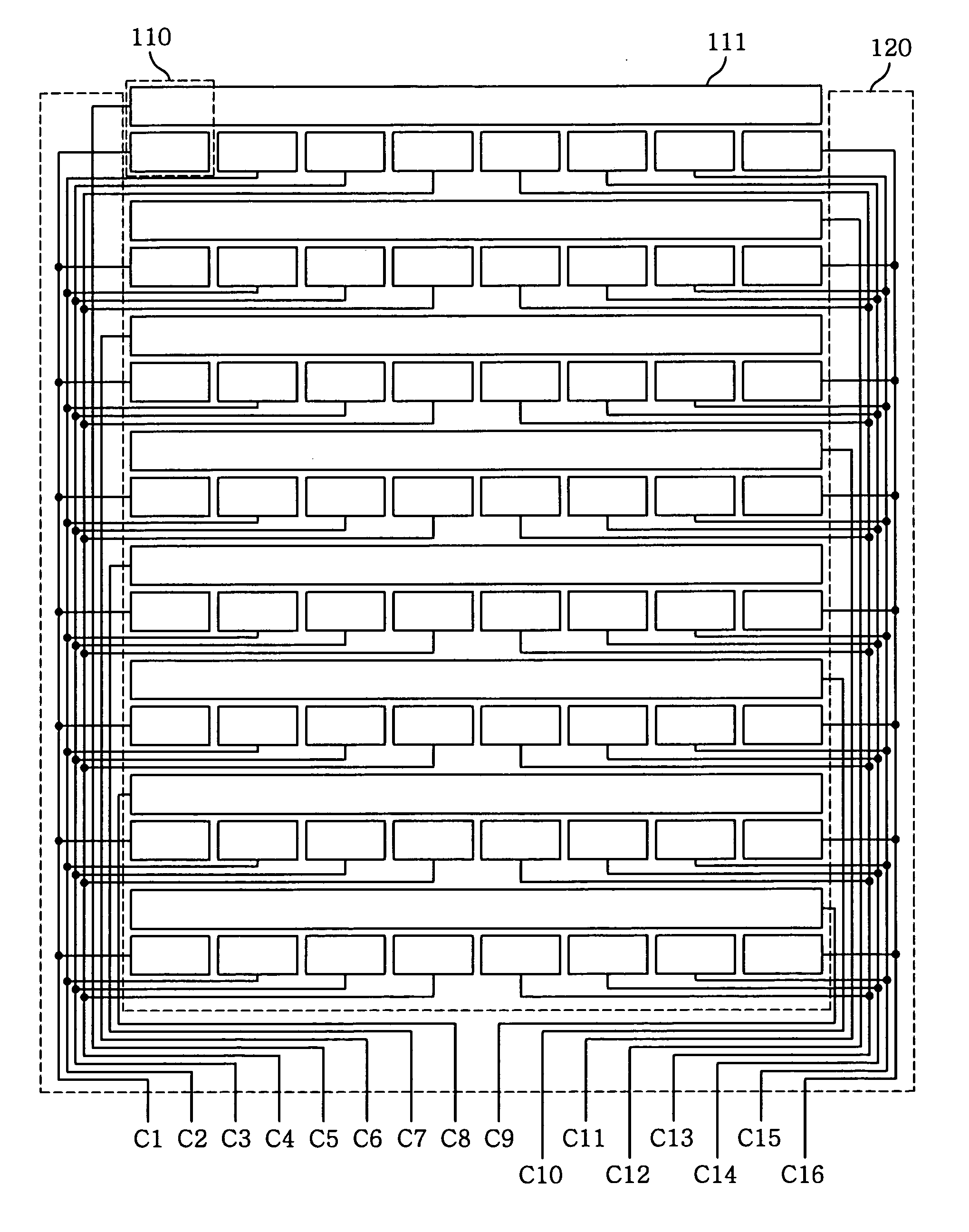
[0025]FIG. 3 illustrates a sensing pattern for detecting a location of a touch on a touch location detecting panel in accordance with a preferred embodiment of the present invention, and FIG. 4 is an enlarged view of a sensing area 110 shown in FIG. 3.

[0026]Referring to FIG. 3, the sensing pattern includes vertical location sensing bars 111 extended in a horizontal direction at a plurality of vertical locations, and horizontal location sensing areas 114 that are arranged at a plurality of horizontal locations in a row adjacently to each of the vertical location sensing bars 111.

[0027]In case of a touch location detecting panel of a capaciti...


PUM


Abstract

The present invention relates to a touch location detecting panel and, more particularly, to a touch location detecting panel having a plurality of sensing areas arranged two-dimensionally. The touch location detecting panel of the invention has on a surface at one side of a single film a plurality of sensing areas arranged two-dimensionally. Each of the sensing areas includes a plurality of partitioned areas electrically isolated from each other, and the partitioned areas are respectively connected to separate channels of a circuit for detecting a user's touch on each of the partitioned areas. Accordingly, durability and productivity of the touch location detecting panel can be improved by simplifying the panel structure.

Description

TECHNICAL FIELD[0001]The present invention relates to a touch location detecting panel applicable to a touch location detecting device such as a touch pad or a touchscreen.BACKGROUND ART[0002]A touch location detecting device is a device for detecting a user's touch at a specific location on a panel that is installed overlappingly on a display screen or provided separately from the display screen. Information on the presence and location of a touch on the panel are utilized for the operation control, screen manipulation and the like of a computer system that incorporates therein the touch location detecting device.[0003]A method for detecting a touch location can be largely classified into two categories: a continuous location detecting type and a discrete location detecting type. The continuous location detecting method or an analog method measures a continuous change in, such as, optical or electrical characteristics caused by a change in user's touch location on a panel, and calc...

Claims


Application Information

Patent Timeline
Patent Type & Authority Applications(United States)
IPC IPC(8): G06F3/044G06F3/041
CPCG06F3/044G06F3/0416G06F3/04164G06F3/0443G06F3/0445G06F3/0446G06F3/0448G06F3/0354G06F3/0412
Inventor BAE, SANG-HO
Owner MELFAS
Why Eureka
Try Eureka