Image sensor and method for manufacturing the same

Inactive Publication Date: 2010-05-06
DONGBU HITEK CO LTD
View PDF4 Cites 3 Cited by
  • Summary
  • Abstract
  • Description
  • Claims
  • Application Information

AI Technical Summary

Benefits of technology

[0005]Embodiments relate to an image sensor, and more particularly, to an image sensor and a method for manufacturing the same that can reduce defects in a microlens. Embodiments relate to the above-mentioned problem and provides an image sen

Problems solved by technology

However, since the photoresist is not very hard and solid, defects may occur in the microlens involving silicon particles generated during wafer sawing.
Meanwhile, since an oxide material formed at lo

Method used


Image

  • Image sensor and method for manufacturing the same
  • Image sensor and method for manufacturing the same
  • Image sensor and method for manufacturing the same

Examples


Example

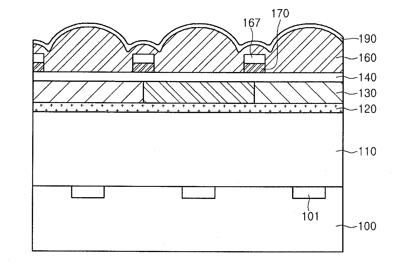
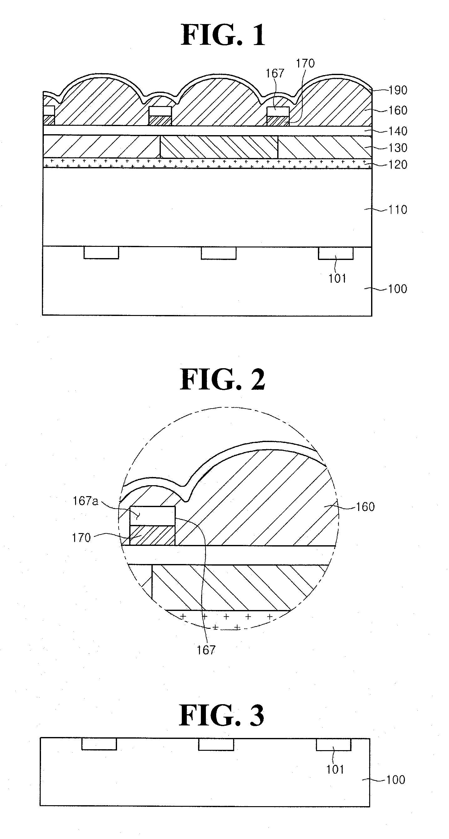
[0013]Example FIG. 1 is a diagram for describing a configuration of an image sensor according to an embodiment and example FIG. 2 is a diagram showing a state where a phase change material is formed at a region between microlenses in detail according to embodiments.

[0014]First, referring to example FIG. 1, the image sensor according to embodiments may include one or more photodiodes 101 that are formed over a semiconductor substrate 100 to generate electric charges depending on the amount of incident light. A dielectric layer 110 may be formed over the semiconductor substrate 100 including the photodiodes 101. A passivation layer 120 may be formed over the dielectric layer 110. An RGB color filter layer 130 may be formed over the passivation layer 120 to transmit light having a predetermined wavelength band. A planarization layer 140 may be formed over the color filter layer 130 that is configured in a convex shape having a predetermined curvature over the planarization layer 140 to...


PUM

PropertyMeasurementUnit
Temperatureaaaaaaaaaa
Areaaaaaaaaaaa
Phaseaaaaaaaaaa

Abstract

An image sensor according to embodiments may include a semiconductor substrate, photodiodes disposed over the semiconductor substrate, a dielectric layer formed over the photodiodes, a color filter layer formed over the dielectric layer, a planarization layer formed over the color filter layer, a phase change material formed over the planarization layer, and a plurality of microlenses formed over the planarization layer, wherein the phase change material is positioned in the microlens. Further, a method for manufacturing an image sensor according to embodiments may include forming a dielectric layer over a semiconductor substrate with a plurality of photodiodes, sequentially forming a color filter layer and a planarization layer over the dielectric layer, forming a phase change material over the planarization layer, forming a patterned phase change material by partially etching the phase change material, and forming microlenses over the planarization layer and the phase change material.

Description

[0001]The present application claims priority under 35 U.S.C. 119 to Korean Patent Application No. 10-2008-0125503 (filed on Dec. 10, 2008), which is hereby incorporated by reference in its entirety.BACKGROUND[0002]Image sensors, as semiconductor devices converting an optical image into an electrical signal, may be largely classified into charge coupled device (CCD) image sensors and complementary metal oxide silicon (CMOS) image sensors. CMOS image sensors capture an image by sequentially detecting and switching electrical signals of unit pixels. A unit pixel may include at least a photodiode and a MOS transistor.[0003]To attain bright and clear image quality in the CMOS image sensor, light should be maximally focused on the photodiode. A microlens, which may be made out of a photoresist, may be used for this. However, since the photoresist is not very hard and solid, defects may occur in the microlens involving silicon particles generated during wafer sawing. To guard against this...

Claims


Application Information

Patent Timeline
IPC IPC(8): H01L47/00H01L31/0232C23F1/08
CPCH01L27/14621H01L27/14627H01L27/14685
Inventor LEE, BYUNG-HO
Owner DONGBU HITEK CO LTD
Why Eureka
Try Eureka