Patterning method
- Summary
- Abstract
- Description
- Claims
- Application Information
AI Technical Summary
Benefits of technology
Problems solved by technology
Method used
Image

Examples
Example
First Embodiment
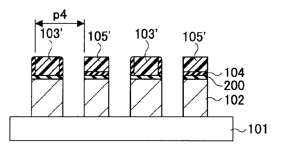
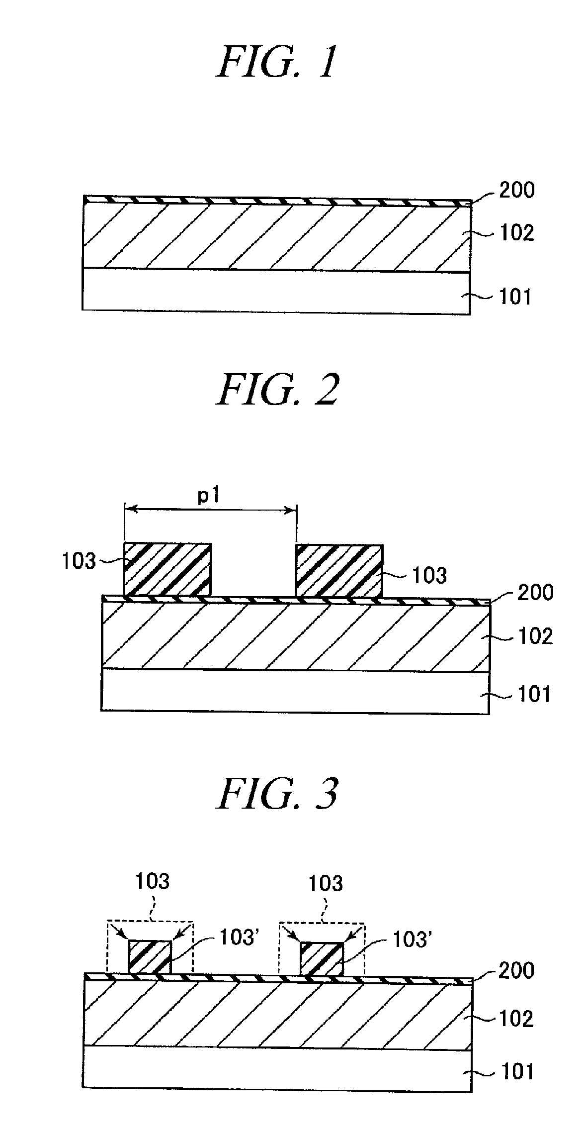
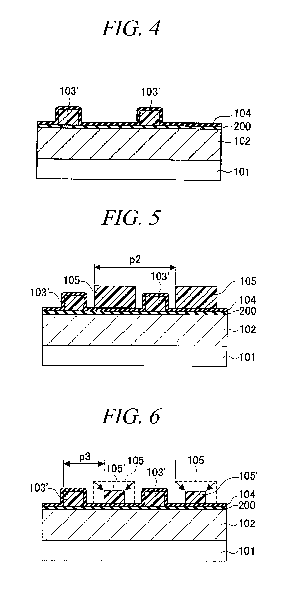
[0063]FIGS. 1 to 6 provide cross sectional views to illustrate every major manufacturing process of a patterning method in accordance with a first embodiment of the present invention.
[0064]The first embodiment illustrates a basic processing sequence of the patterning method in accordance with the present invention.
[0065]First, as shown in FIG. 1, a thin film 102 is formed on a semiconductor substrate 101. In the present specification, the semiconductor substrate 101 does not merely imply a semiconductor substrate, e.g., a silicon substrate, but includes a structure body having, in or on the semiconductor substrate, a semiconductor device, a conductive film corresponding to an integrated circuit pattern and an interlayer insulating film which insulates them. The thin film 102 is a film to be processed into a micro pattern later, and it may be an insulating film made of SiN or SiO2, or a conductive film such as conductive polysilicon. In the present embodiment, the thi...
Example
Second Embodiment
[0124]FIG. 13 provides a cross sectional view to describe a major manufacturing process of a patterning method in accordance with a second embodiment of the present invention.
[0125]As illustrated in FIG. 13, in the second embodiment, the first trimming process and the hardening process as described in the first embodiment are performed consecutively in the same film forming apparatus (in-situ process).
[0126]The trimming process is performed by using an etching apparatus or an ashing apparatus, while the hardening process is performed by using a film forming apparatus. For this reason, in general, after the trimming process is finished, a semiconductor substrate (wafer) is taken out of the ashing apparatus first, and then transferred to the film forming apparatus.
[0127]In this manner, since the wafer is taken out of the apparatus after the trimming process, there is a possibility that dust or the like is adhered to a surface of a resist pattern 103′. If the dust or t...
Example
Third Embodiment
[0135]FIGS. 15 to 23 provide cross sectional views to illustrate every major manufacturing process of a patterning method in accordance with a third embodiment of the present invention.
[0136]The third embodiment illustrates an example of the patterning method in accordance with the present invention which can be more appropriately applied to an actual semiconductor process.
[0137]First, as illustrated in FIG. 15, a thin film 102, e.g., a conductive silicon film is formed on a semiconductor substrate 101, and then a hard mask film 106 is formed on the thin film 102 in the same manner as the first embodiment. The hard mask film 106 is made of a film different from the thin film 102 and is made of a film capable of obtaining an etching selectivity with respect to the thin film 102. For example, in case the thin film 102 is the conductive silicon film, a silicon nitride film may be selected as the hard mask film 106. Subsequently, a bottom anti-reflection coating 200 is f...
PUM
 Abstract
Description
Claims
Application Information
 - R&D Engineer
- R&D Manager
- IP Professional
- Industry Leading Data Capabilities
- Powerful AI technology
- Patent DNA Extraction
Browse by: Latest US Patents, China's latest patents, Technical Efficacy Thesaurus, Application Domain, Technology Topic.
© 2024 PatSnap. All rights reserved.Legal|Privacy policy|Modern Slavery Act Transparency Statement|Sitemap