
Method of manufacturing semiconductor device in which bottom surface and side surface of semiconductor substrate are covered with resin protective film

Inactive Publication Date: 2010-06-10
TERAMIKROS INC
View PDF7 Cites 0 Cited by
  • Summary
  • Abstract
  • Description
  • Claims
  • Application Information

AI Technical Summary

Benefits of technology

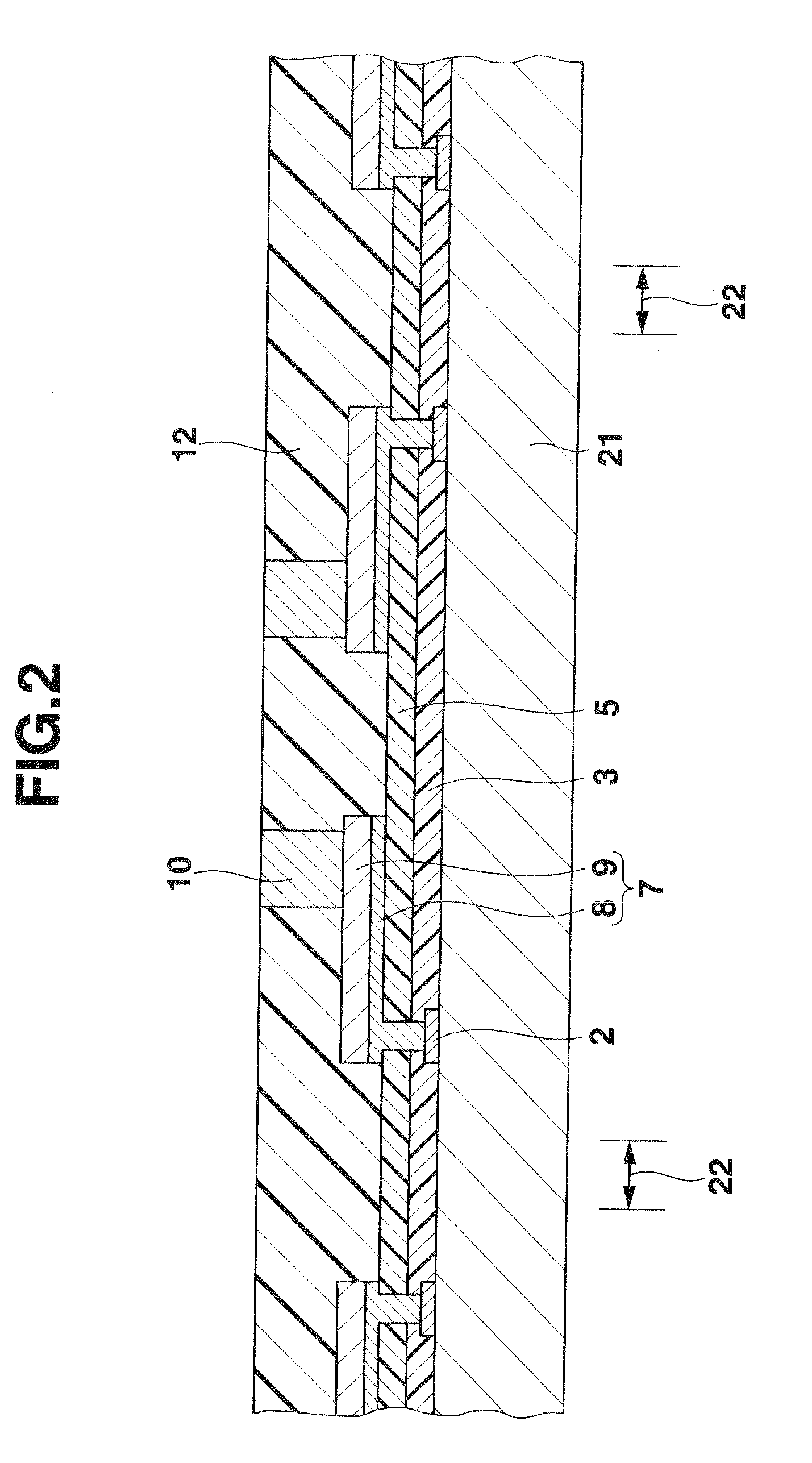
[0011]According to this invention, a resin protective film is formed on the bottom surface of a semiconductor wafer (semiconductor substrates) including the inner part of a trench in a condition where a support plate is affixed to an external connection bump electrode and a sealing film. Thus, it is possible to prevent the entirety including the semiconductor substrates from being easily warped during the formation of the resin protective film for protecting the semiconductor substrates.

Problems solved by technology

This disadvantageously causes difficulty in maintaining the quality and in handling in each step.

Method used


Image

  • Method of manufacturing semiconductor device in which bottom surface and side surface of semiconductor substrate are covered with resin protective film
  • Method of manufacturing semiconductor device in which bottom surface and side surface of semiconductor substrate are covered with resin protective film
  • Method of manufacturing semiconductor device in which bottom surface and side surface of semiconductor substrate are covered with resin protective film

Examples


Embodiment Construction

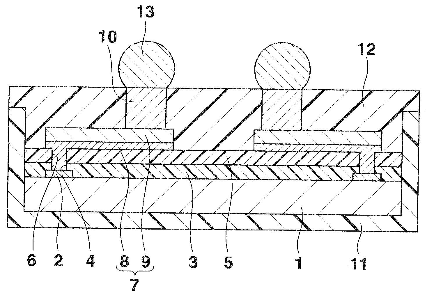
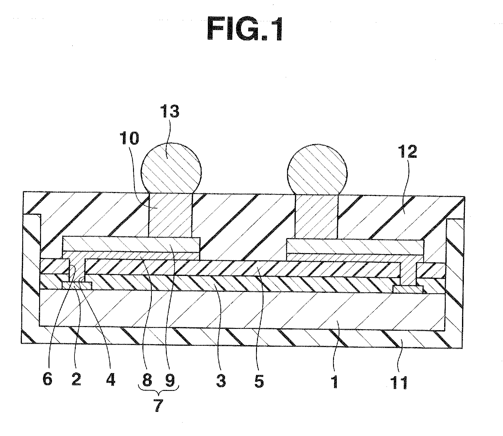
[0029]FIG. 1 shows a sectional view of one example of a semiconductor device manufactured by a manufacturing method of this invention. This semiconductor device is generally called a CSP, and includes a silicon substrate (semiconductor substrate) 1. Elements (not shown) constituting an integrated circuit having a predetermined function, such as a transistor, a diode, a register and a condenser, are formed on the upper surface of the silicon substrate 1. Connection pads 2 made of, for example, an aluminum-based metal and connected to the elements of the integrated circuit are provided in the peripheral part of the upper surface of the silicon substrate 1. Although two connection pads 2 are only shown, a large number of connection pads 2 are actually arranged on the peripheral part of the upper surface of the silicon substrate 1.

[0030]A passivation film (insulating film) 3 of, for example, silicon oxide is provided on the upper surfaces of the silicon substrate 1 except for the center...


PUM


Abstract

First, a trench formed in parts of a semiconductor wafer, a sealing film and others corresponding to a dicing street and both sides thereof. In this state, the semiconductor wafer is separated into silicon substrates by the formation of the trench. Then, a resin protective film is formed on the bottom surface of each silicon substrate including the inner part of the trench. In this case, the semiconductor wafer is separated into the silicon substrates. However, a support plate is affixed to the upper surfaces of the columnar electrode and the sealing film via an adhesive layer. Therefore, when the resin protective film is formed, it is possible to prevent the entirety including the separated silicon substrates from being easily warped.

Description

CROSS-REFERENCE TO RELATED APPLICATIONS[0001]This application is based upon and claims the benefit of priority from prior Japanese Patent Application No. 2008-314022, filed Dec. 10, 2008, the entire contents of which are incorporated herein by reference.BACKGROUND OF THE INVENTION[0002]1. Field of the Invention[0003]The present invention relates to a method of manufacturing a semiconductor device in which the bottom surface and side surface of a semiconductor substrate are covered with a resin protective film.[0004]2. Description of the Related Art[0005]A device which is called a chip-size package (CSP) is known from Published Japanese Patent No. 4103896. In this semiconductor device, a plurality of wiring lines are provided on the upper surface of an insulating film disposed on a semiconductor substrate. A columnar electrode is provided on the upper surface of a connection pad portion of the wiring line. A sealing film is provided on the upper surface of the insulating film includi...

Claims


Application Information

Patent Timeline
IPC IPC(8): H01L21/50
CPCH01L21/568H01L2924/01047H01L21/78H01L23/3114H01L23/3135H01L24/03H01L24/05H01L24/11H01L24/13H01L24/19H01L24/94H01L2221/6834H01L2224/16H01L2224/18H01L2224/94H01L2924/01012H01L2924/01013H01L2924/01029H01L2924/01033H01L2924/09701H01L2924/14H01L2924/19041H01L21/6836H01L2924/01006H01L2224/11H01L2224/03H01L2224/0401H01L2924/3511H01L2224/023H01L2924/0001H01L23/28
Inventor KOROKU, TAISUKEOKADA, OSAMUKUWABARA, OSAMUSHIOTA, JUNJIFUJII, NOBUMITSU
Owner TERAMIKROS INC
Learn More