Light-emitting device

a technology of light-emitting devices and components, applied in semiconductor devices, diodes, electrical apparatus, etc., can solve the problems of generating noise, unable to obtain sufficient light output from leds, and generating components of speck noise, so as to reduce speck noise, reduce noise, and increase output

Active Publication Date: 2010-06-24
SEIKO EPSON CORP
View PDF17 Cites 22 Cited by
  • Summary
  • Abstract
  • Description
  • Claims
  • Application Information

AI Technical Summary

Benefits of technology

[0017]In the structure above, laser oscillation of light generated in the gain region can be suppressed or prevented in the manner described below. Therefore, speckle noise can be reduced. With the light-emitting device of the present invention, the light generated in the gain region advances while increasing gain in the gain region and can be emitted to the exterior. Therefore, a higher output than a conventional LED can be obtained. As described above, speckle noise can be reduced, and a novel, high-output light-emitting device can be provided in accordance with the present invention.

Problems solved by technology

However, speckle noise components generated when randomly reflected rays of light at the screen surface interfere with each other.
However with the method disclosed in Japanese Laid-open Patent Application No. 11-64789, there are cases in which new problems arise; i.e., the screen is limited, a motor and other components are required to move the screen, and the motor or the like generate noise.
However, sufficient light output cannot be obtained using an LED.

Method used


Image

  • Light-emitting device
  • Light-emitting device
  • Light-emitting device

Examples


first embodiment

[0049]1.1. The light-emitting device 100 of the first embodiment will be described first.

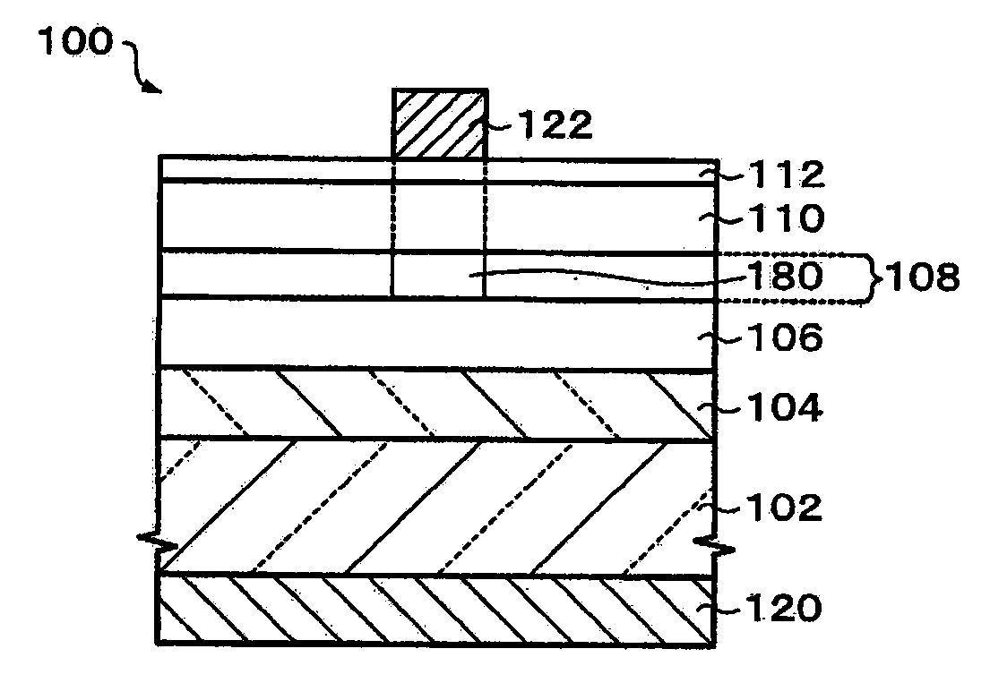
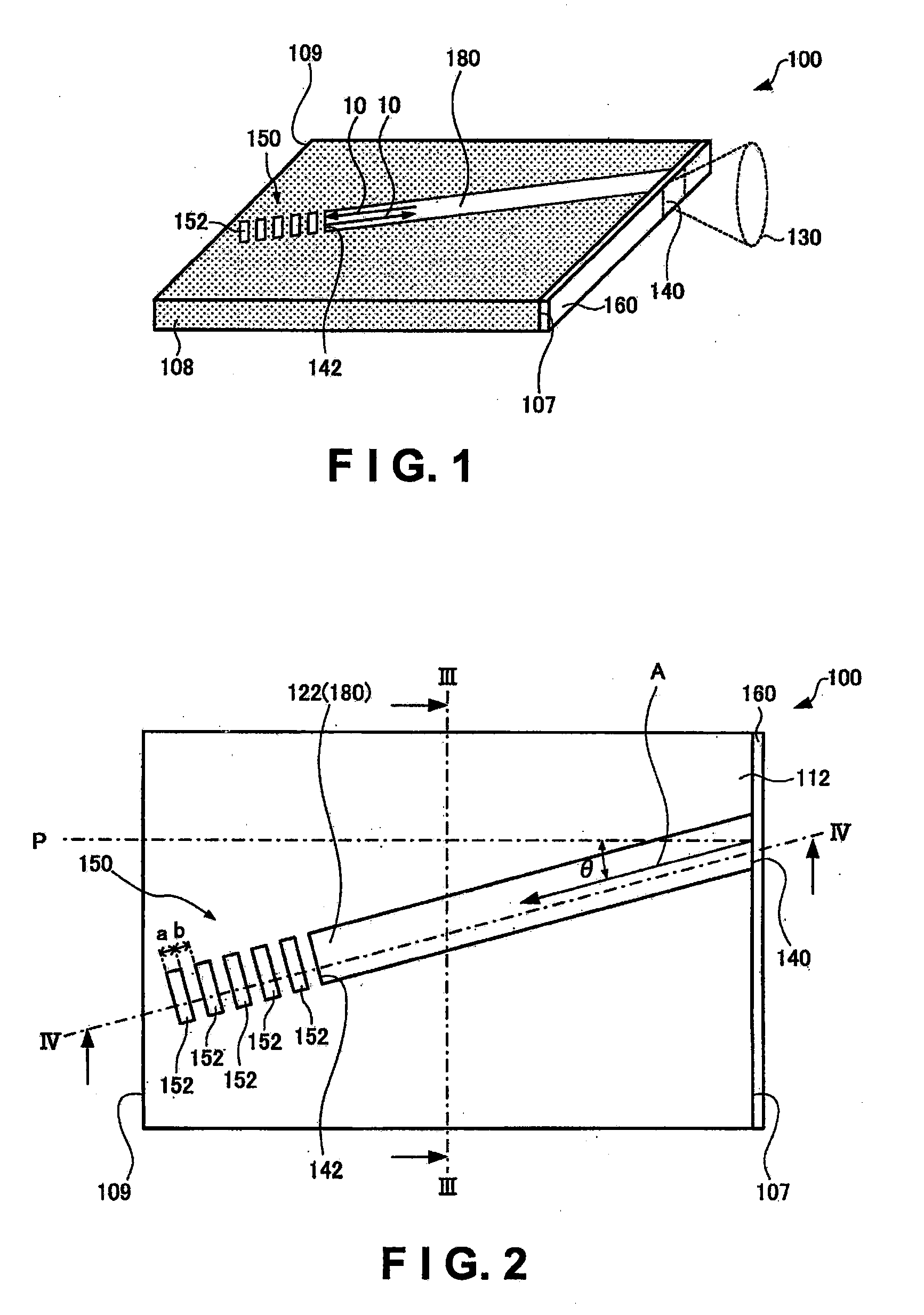
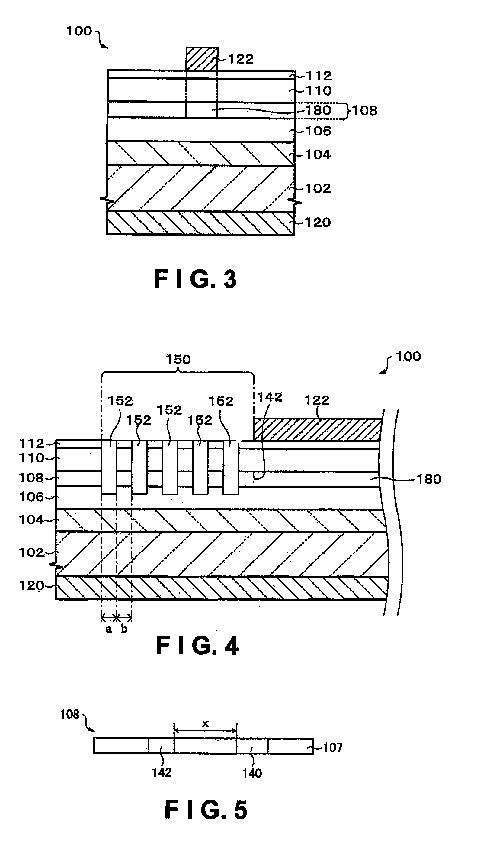
[0050]FIG. 1 is a perspective view schematically showing the light-emitting device 100. FIG. 2 is a plan view schematically showing the light-emitting device 100. FIG. 3 is a cross-sectional view along the line III-III of FIG. 2. FIG. 4 is a cross-sectional view along the line IV-IV of FIG. 2. In FIG. 1, members other than the active layer 108, the reflective part 150, and the antireflective film 160 are omitted from the drawing for the sake of convenience. Described here is the case in which the light-emitting device 100 is an InGaAlP-type (red) semiconductor light-emitting device.

[0051]The light-emitting device 100 includes a first cladding layer 106, an active layer 108, a second cladding layer 110, and a reflective part 150, as shown in FIGS. 1 to 4. The light-emitting device 100 may further include, e.g., a first electrode 120, a second electrode 122, a substrate 102, a buffer layer 104, a ...

second embodiment

2. Second Embodiment

[0111]2.1. Next, the light-emitting device 700 of the second embodiment will be described next, but no limitation is imposed by the following example.

[0112]FIG. 13 is a plan view schematically showing the light-emitting device 700, and FIG. 14 is a cross-sectional view along the line XIV-XIV. In the light-emitting device 700 of the second embodiment, the same reference numerals are used for members having the same function as the constituent elements of the light-emitting device 100 of the first embodiment described above, and a detailed described thereof is omitted.

[0113]The light-emitting device 700 has a first cladding layer 106, an active layer 108, a second cladding layer 110, insulating parts 702, and a reflective part 150, as shown in FIGS. 13 and 14. The light-emitting device 700 may further include, e.g., a first electrode 120, a second electrode 122, a substrate 102, a buffer layer 104, a contact layer 112, and an antireflective film 160.

[0114]In the ex...


PUM


Abstract

The light-emitting device 100 of the present invention has a first cladding layer 106; an active layer 108 formed above the first cladding layer 106; and a second cladding layer 110 formed above the active layer 108, wherein the active layer 108 has a first side surface 107, and a second side surface 109 parallel to the first side surface 107; at least a portion of the active layer 108 constitutes a gain region 180; the gain region 180 has a first end surface 140 disposed on the first side surface 107 side and a second end surface 142 disposed on the second side surface 109 side, and extends from the first end surface 140 to the second end surface 142 in the direction inclined to the normal to the first side surface 107 as viewed from above; the second end face 109 is orthogonal to the direction in which the gain region 180 extends as viewed from above; a reflecting part 150 is disposed on the second end face 109; and a part of the light 10 generated in the gain region 180 is reflected in the reflecting part 150 disposed on the second end face 142 and is emitted from the first end surface 140.

Description

CROSS-REFERENCE TO RELATED APPLICATION[0001]This application is based on and claims priority from Japanese Patent Application No. 2008-324291, filed on Dec. 19, 2008, the contents of which are incorporated herein by reference.BACKGROUND[0002]1. Technical Field[0003]The present invention relates to a light-emitting device.[0004]2. Related Art[0005]High-intensity laser devices having excellent color reproducibility show great promise as light-emitting devices that serve as a light source for projectors, displays, and other display devices. However, speckle noise components generated when randomly reflected rays of light at the screen surface interfere with each other. In response to this problem, Japanese Laid-open Patent Application No. 11-64789, for example, proposes a method for reducing speckle noise by sliding the screen to vary the speckle pattern.[0006]However with the method disclosed in Japanese Laid-open Patent Application No. 11-64789, there are cases in which new problems ...

Claims


Application Information

Patent Timeline
Patent Type & Authority Applications(United States)
IPC IPC(8): H01L33/00
CPCH01L33/0045H01L33/14H01L33/10H01L33/46H01L33/20
Inventor NAGAWA, MICHIFUMI
Owner SEIKO EPSON CORP
Why Eureka
Try Eureka