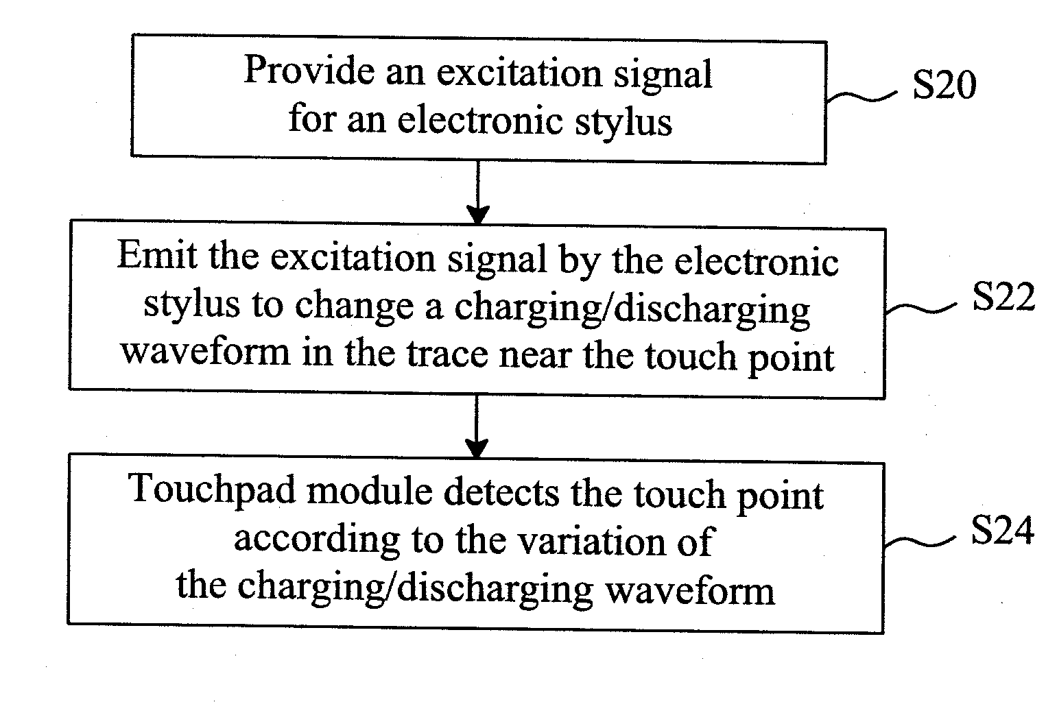
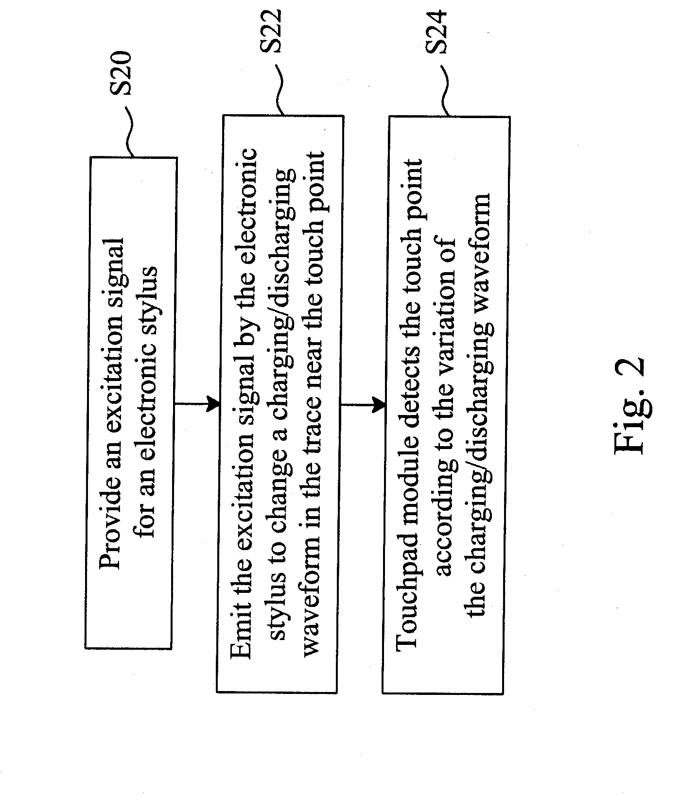
Electronic stylus, capacitive touchpad module, and apparatus for touch input
a capacitive touchpad and electronic stylus technology, applied in the field of electronic stylus for capacitive touchpad module, can solve the problems of inability to induce a sufficient capacitance variation of the trace of the stylus, and the thickness of the finger is too larg
- Summary
- Abstract
- Description
- Claims
- Application Information
AI Technical Summary
Benefits of technology
Problems solved by technology
Method used
Image

Examples
first embodiment
[0050]FIG. 10 is a diagram showing a wireless apparatus for touch input according to the present invention. In this embodiment, the capacitive touchpad module 14 includes an FPC board 90, or may be the same PCB on a substrate 96, a detection circuit 92 and an up-converter circuit 93 are disposed on the FPC board 90, the detection circuit 92 is connected to the up-converter circuit 93 and the substrate 96 through conductive wires, the substrate 96 may be a glass plate, a plastic membrane, or a PCB, and traces 98, which may be made from an ITO thin film or another kind of conductor, are printed on the substrate 96. The capacitive touchpad module 14 charges / discharges the traces 68 at a charging / discharging frequency one by one sequentially, and each of the traces 68 will generate a charging / discharging signal, through a respective conductive wire 94, for the detection circuit to generate a detection signal Sd1 whose frequency is up-converted by the up-converter circuit 93 to generate ...
second embodiment
[0052]FIG. 12 is a diagram showing a wireless apparatus for touch input according to the present invention. In this embodiment, in addition to most of the elements shown in FIG. 10, it is a modulation circuit 95 to modulate the detection signal Sd1 to generate a carrier Sd3 which is then transmitted by the wireless transceiver system 100 to the electronic stylus 12 where the carrier Sd3 is demodulated into the excitation signal Srf. In other embodiments, the modulation circuit 95 may also incorporate the detection signal Sd1 or the charging / discharging signal detected from the conductive wire 94 as data into the carrier Sd3 for transmission to the electronic stylus 12, so that the data carried by the carrier Sd3 can be unpacked through demodulation by the electronic stylus 12 to generate the excitation signal Srf according to the data.
[0053]FIG. 13 is a diagram showing an embodiment for the electronic stylus 12 of FIG. 12, in which it is a demodulation circuit 118 to demodulate the ...
PUM
 Abstract
Description
Claims
Application Information
 - R&D
- Intellectual Property
- Life Sciences
- Materials
- Tech Scout
- Unparalleled Data Quality
- Higher Quality Content
- 60% Fewer Hallucinations
Browse by: Latest US Patents, China's latest patents, Technical Efficacy Thesaurus, Application Domain, Technology Topic, Popular Technical Reports.
© 2025 PatSnap. All rights reserved.Legal|Privacy policy|Modern Slavery Act Transparency Statement|Sitemap|About US| Contact US: help@patsnap.com