Semiconductor laser apparatus

a laser and semiconductor technology, applied in the direction of semiconductor lasers, lasers, solid-state devices, etc., can solve the problems of large stress generation on the semiconductor laser device, large shrinkage difference between the semiconductor laser device and the heat dissipating member, etc., to achieve high heat emission efficiency, suppress the generation of stress in the semiconductor laser device during bonding, and reduce the effect of heat emission

Inactive Publication Date: 2010-07-29
SONY CORP
View PDF1 Cites 0 Cited by
  • Summary
  • Abstract
  • Description
  • Claims
  • Application Information

AI Technical Summary

Benefits of technology

[0012]In the semiconductor laser apparatus according to an embodiment of the present invention, the semiconductor laser device is bonded along the front end portion of the main body of the heat dissipating member while the pair of protruding portions are disposed on both sides of the front end portion, the protruding portion...

Problems solved by technology

However, in the method disclosed in Japanese Unexamined Patent Application Publication No. 2007-305977, a stress can be relaxed due to the bridged structure without decreasing the efficiency of heat emission, but the method poses a problem in that a deformation such as warpage is caused on a semiconductor laser.
There is normally a large difference in a coefficient of linea...

Method used


Image

  • Semiconductor laser apparatus
  • Semiconductor laser apparatus
  • Semiconductor laser apparatus

Examples


modification 1

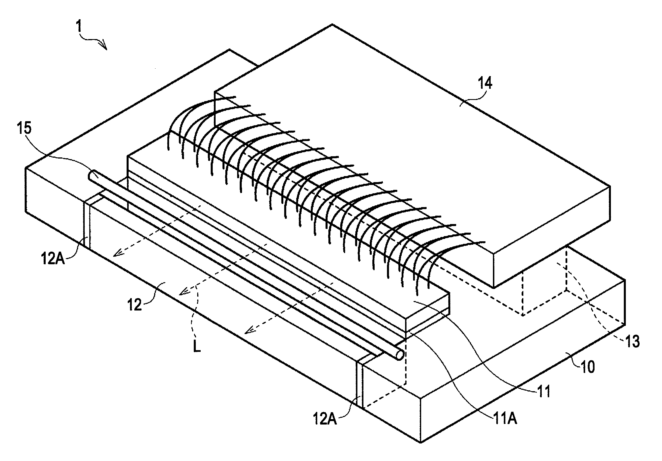
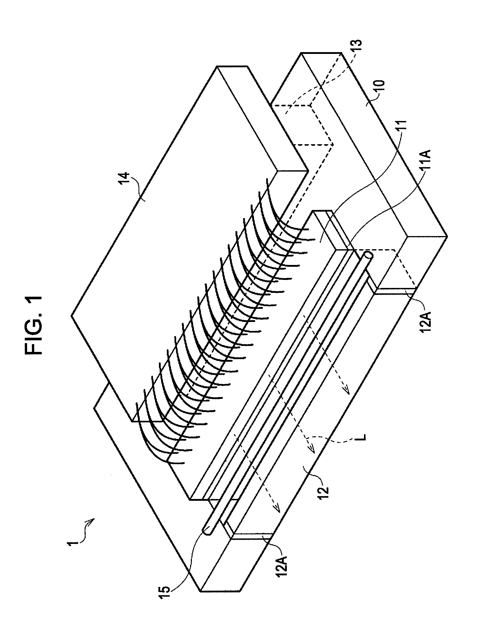
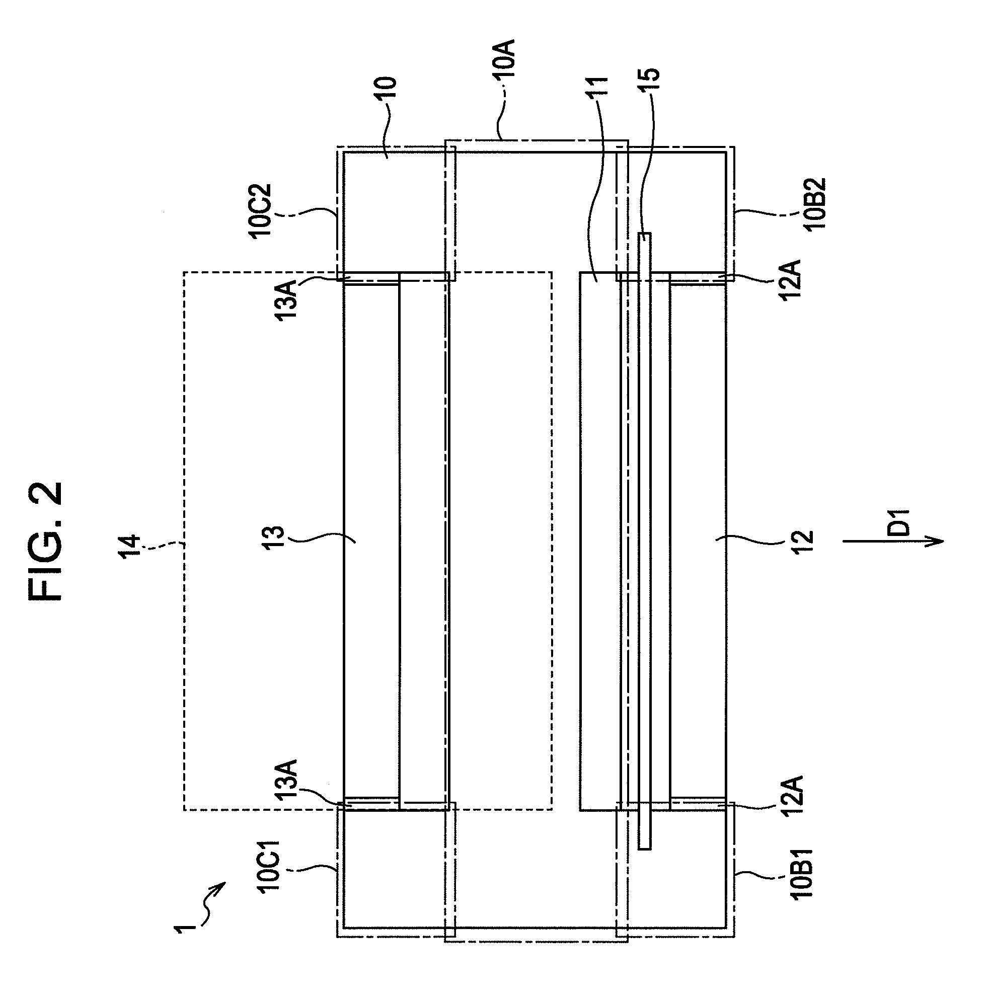
[0052]FIG. 5 shows a schematic structure of a semiconductor laser apparatus 2 according to a modification 1. The semiconductor laser apparatus 2 has the same structure as in the above-described embodiment except metal layers 12B that bond the stiffener 12 to the pair of protruding portions 1081 and 10B2 of the heat sink 10 and metal layers 13B that bond the stiffener 13 to the pair of protruding portions 10C1 and 10C2. The metal layers 12B and 13B are composed of a material having a higher melting point than the metal layer 11A, for example, a bonding metal having a melting point of about 750° C. or less such as a brazing filler metal. Such metal layers 12B and 13B are composed of tin-phosphor copper or the like.

[0053]For example, the semiconductor laser apparatus 2 can be manufactured as follows. First, a semiconductor laser array 11 is manufactured as in the semiconductor laser apparatus 1 of the embodiment described above. The metal layers 12B and 13B composed of, for example, th...


PUM


Abstract

A semiconductor laser apparatus includes a heat dissipating member including a main body having a front end portion that extends in a left-right direction and a pair of protruding portions that protrude forward from both sides of the front end portion; a semiconductor laser device bonded along the front end portion of the main body; and a stiffener configured to bridge the pair of protruding portions.

Description

BACKGROUND OF THE INVENTION[0001]1. Field of the Invention[0002]The present invention relates to a semiconductor laser apparatus obtained by mounting a semiconductor laser device on a heat dissipating member such as a heat sink. 2. Description of the Related Art[0003]In apparatuses for which semiconductor lasers are used, a problem related to generation of heat has become serious, which limits the application of semiconductor lasers in various fields. This problem concerns generated heat per unit area in semiconductor lasers and causes phenomena such as a temperature increase around a semiconductor laser and generation of stress due to thermal cycling. Such phenomena decrease the light-emitting output and light-emitting efficiency of semiconductor lasers and shorten the life thereof. Furthermore, such phenomena degrade laser characteristics, that is, light emitted from semiconductor lasers is shifted to longer wavelengths. Therefore, in apparatuses to which semiconductor lasers are ...

Claims


Application Information

Patent Timeline
IPC IPC(8): H01S5/024H01S3/04H01S5/023H01S5/0233
CPCH01S5/005H01S5/02272H01S5/024H01S5/02236H01S5/4025H01S5/02252H01S5/02492H01L2224/48091H01L2224/49175H01S5/023H01S5/0233H01S5/0235H01S5/02326H01S5/0237H01L2924/00014
Inventor WAKABAYASHI, KAZUYAIMANISHI, DAISUKE
Owner SONY CORP
Why Eureka
Try Eureka