
Liquid crystal display device and method of manufacturing same

a technology of liquid crystal display and liquid crystal, which is applied in the direction of optics, instruments, non-linear optics, etc., can solve the problems of degrading display quality and yield in production, and achieve the effect of high display quality

Inactive Publication Date: 2010-08-12
SHARP KK
View PDF7 Cites 2 Cited by
  • Summary
  • Abstract
  • Description
  • Claims
  • Application Information

AI Technical Summary

Benefits of technology

[0026]The present invention surely makes luminance point defects invisible and therefore provides a liquid crystal display device having high display quality.

Problems solved by technology

These spots would be detected as luminance point defects, and greatly degrade the display quality and yield in production.

Method used


Image

  • Liquid crystal display device and method of manufacturing same
  • Liquid crystal display device and method of manufacturing same
  • Liquid crystal display device and method of manufacturing same

Examples


Embodiment Construction

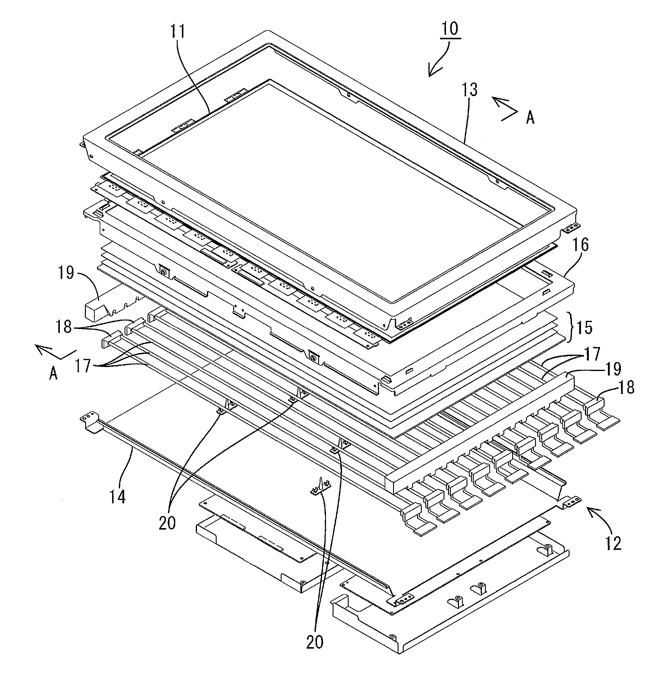
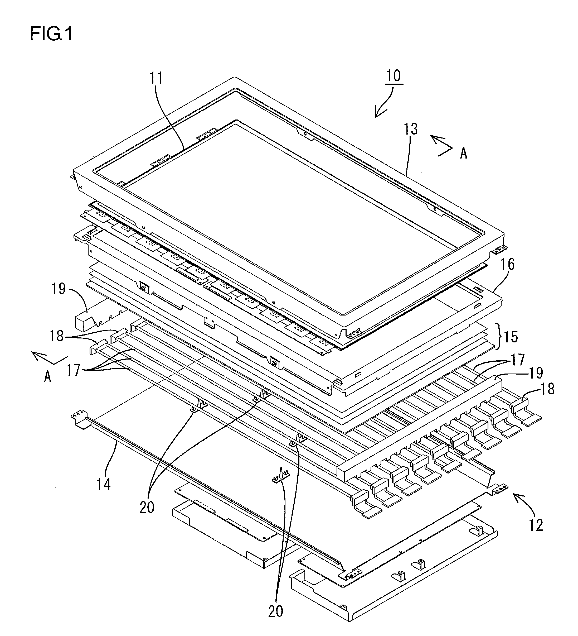
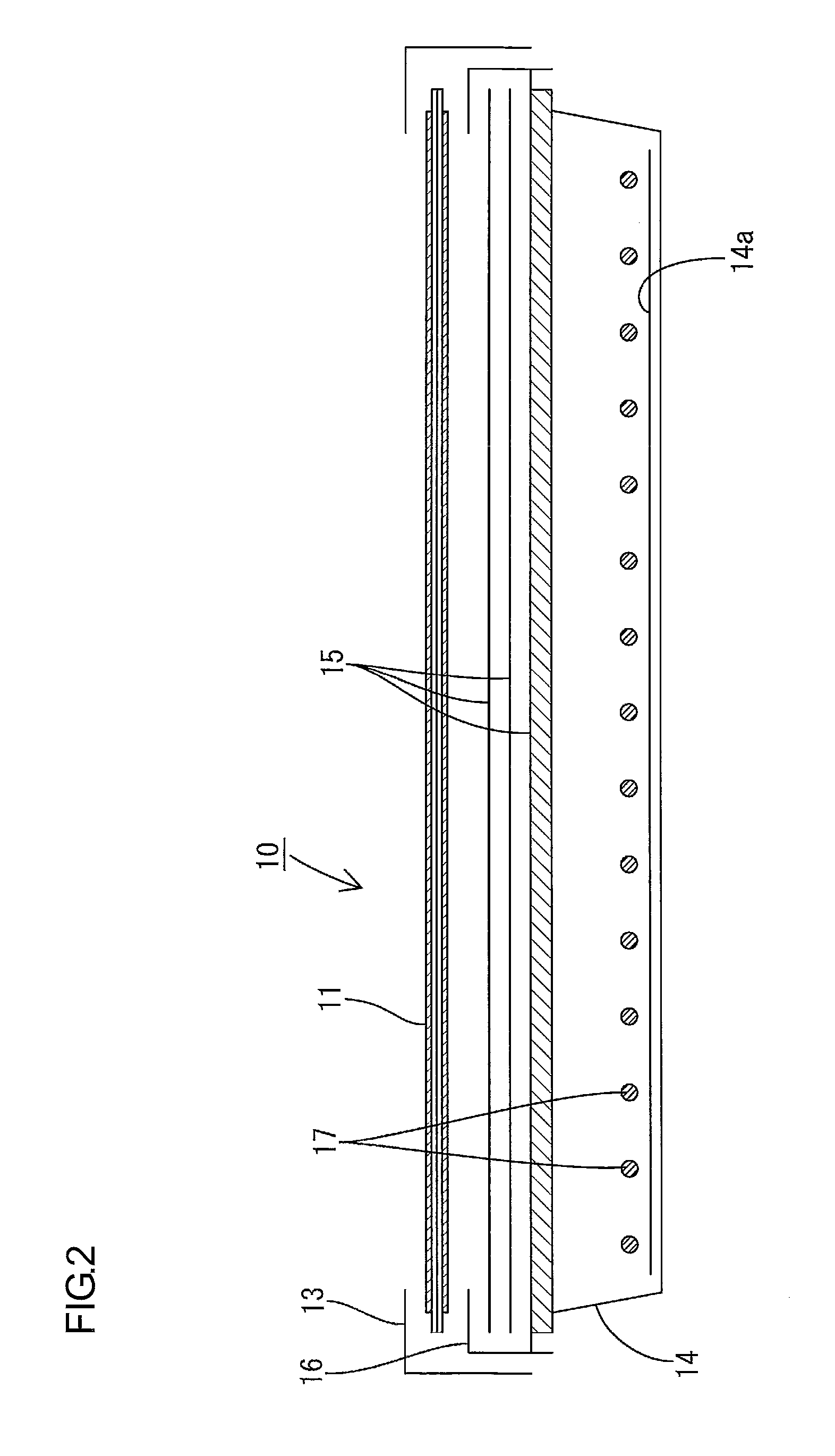
[0034]An embodiment of the present invention will be explained with reference to FIGS. 1 to 6.

[0035]FIG. 1 is a perspective view showing a general construction of a liquid crystal display device according to this embodiment. FIG. 2 is a cross-sectional view of the liquid crystal display device shown in FIG. 1 cut with an A-A line. FIG. 3 is a cross-sectional view of a main part of a liquid crystal panel included in the liquid crystal display device shown in FIG. 1. FIG. 4 is an explanatory view showing operational effect of the liquid crystal display device according to this embodiment. FIG. 5 is an explanatory view showing an embodiment of lighting inspection process for an inspection liquid crystal panel. FIG. 6 is a side view showing a general construction of a luminance point defect compensation device.

[0036]An overall construction of a liquid crystal display device 10 according to the present embodiment will be explained. The liquid crystal display device 10, as shown in FIGS. ...


PUM

PropertyMeasurementUnit
wavelengthaaaaaaaaaa
wavelength rangeaaaaaaaaaa

Abstract

A liquid crystal display device 10 of the present invention includes a liquid crystal panel 11 and a lighting device 12. The liquid crystal panel 11 has a liquid crystal layer 50 between a pair of glass substrates 31 and 41. The lighting device 12 supplies illumination light to the liquid crystal panel 11. The glass substrate 31 at least has a colored portion including a nonbridging oxygen hole center in an area that can block light to luminance defect area X that is a possible cause of a luminance point defect.

Description

TECHNICAL FIELD[0001]The present invention relates to a liquid crystal display device and a method of manufacturing the liquid crystal display device.BACKGROUND ART[0002]The following is an example of method of manufacturing a liquid crystal display device. Switching elements (e.g., TFT) and pixel electrodes are arranged on one of glass substrates provided in a pair, and counter electrodes are arranged on the other glass substrate. Those glass substrates are then bonded with spacers between them. Liquid crystal is disposed between the glass substrates so as to form a liquid crystal layer. Polarizing plates are attached to respective surfaces of the glass substrates, and then a liquid crystal panel is produced. A lighting device that has a plurality of cold cathode tubes as light source is mounted to the liquid crystal panel.[0003]In such a production process of liquid crystal display device, a defect detection using various inspections may be performed at a predetermined point. In a...

Claims


Application Information

Patent Timeline
Patent Type & Authority Applications(United States)
IPC IPC(8): G02F1/13357G02F1/13
CPCC03C23/0025G02F1/1303G02F2202/09G02F2201/508G02F1/1309
Inventor IKEDA, MASAKI
Owner SHARP KK
Learn More