Cache memory

a memory and cache technology, applied in the field of cache memory, can solve the problems of system failure, process variation on the rise, unpunctual access time and inability to read/write, etc., and achieve the effect of minimizing access failure and reducing access time delay in word lines

Active Publication Date: 2010-08-19
KOREA UNIV RES & BUSINESS FOUND
View PDF2 Cites 1 Cited by
  • Summary
  • Abstract
  • Description
  • Claims
  • Application Information

AI Technical Summary

Benefits of technology

[0009]Accordingly, an aspect of the present invention is to provide a cache memory, in which a word-line voltage control logic unit and a word-line driver are added as a logic circuit between a low decoder and a word line, so that a reinforcement voltage signal having a higher level than a basic voltage signal can be applied when accessing the word line corresponding to an access time failure, thereby decreasing an access time delay in the word line in order to minimize an access failure to the cache memory due to process variation.

Problems solved by technology

As the size of a transistor used in a chip becomes smaller, a problem of process variation has been on the rise.
Accordingly, in the case of a 6-transistors static random-access memory (6T SRAM) cell generally used in a cache memory, if six transistors are a little different in characteristics, two problems may arise.
Specifically, it may be unpunctual in an access time and unable to read / write.
Such problems may cause the whole of a cache line having a defect to be unable, and bring a system failure in the case of a direct-mapped cache.
In even the case of a set-associative cache, it is impossible to use all ways, thereby causing damage in performance.
In result, there is an unusable cache line owing to the foregoing defect, and thus a yield of the cache memory decreases.
Particularly, an access failure due to the unpunctual access time is far more likely to occur than unstable reading / writing.

Method used


Image

  • Cache memory
  • Cache memory
  • Cache memory

Examples


Embodiment Construction

[0023]Below, a cache memory according to an exemplary embodiment of the present invention will be described with reference to accompanying drawings.

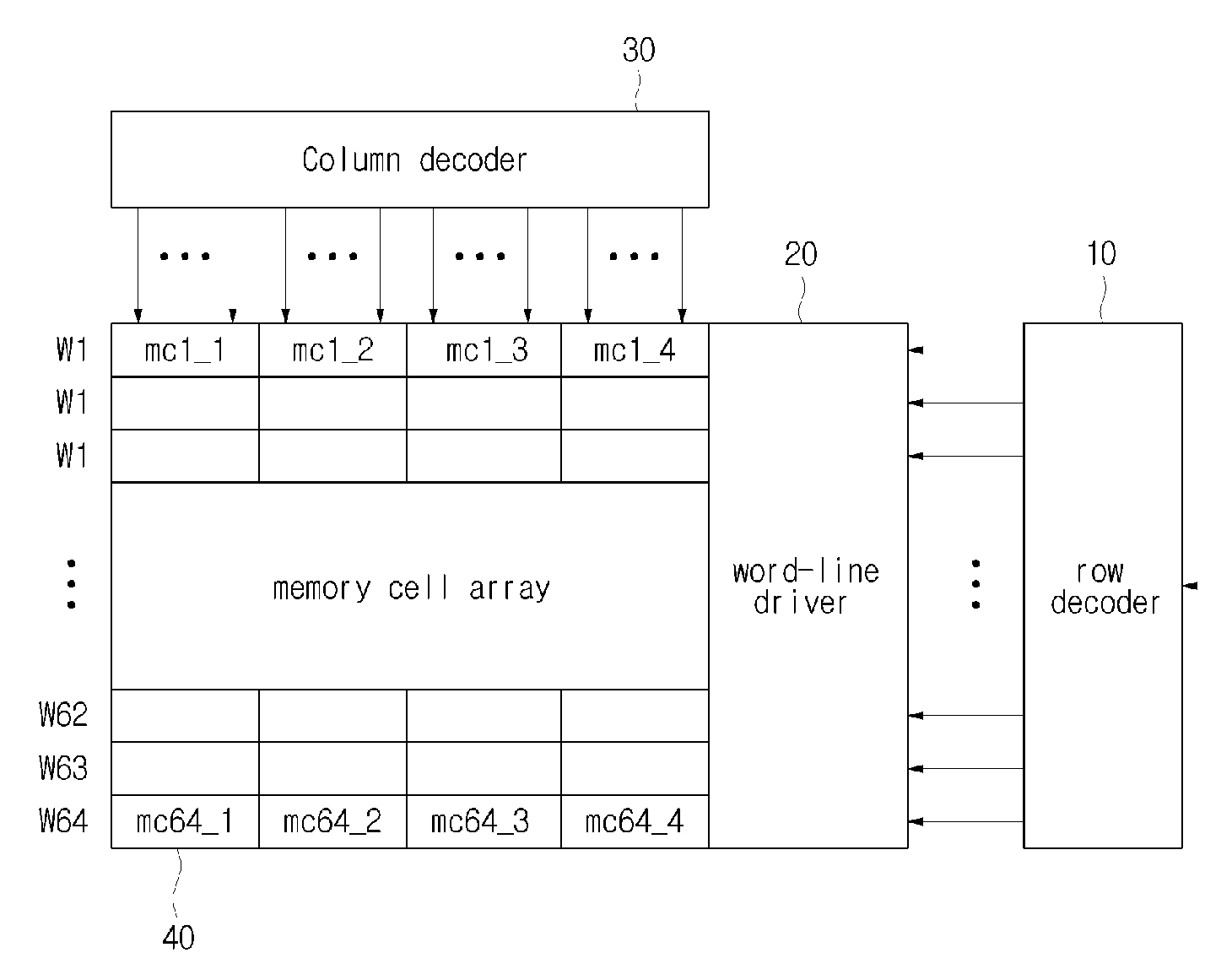
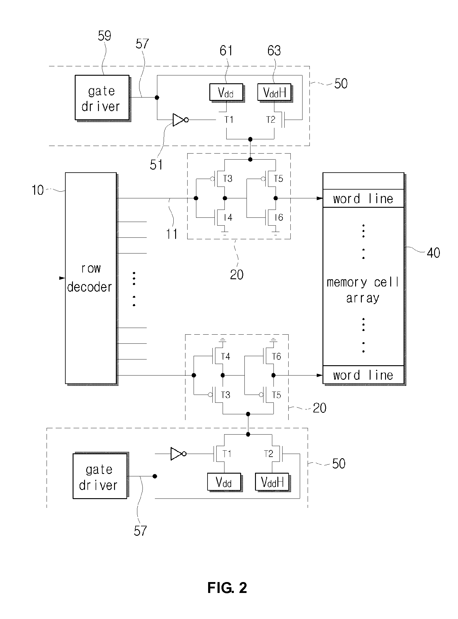
[0024]FIG. 1 is a schematic view of a general cache memory, and FIG. 2 is a schematic view of a modified cache memory applied to an embodiment of the present invention.

[0025]As shown therein, a general cache memory includes a row decoder 10, a word-line driver 20, a column decoder 30, and a memory cell array 40.

[0026]The row decoder 10 decodes and outputs a row address signal received from an external unit (not shown). The decoded signal is used in controlling the word-line driver 20. On the basis of the decoded signal, the word-line driver 20 activates some word lines included in the memory cell array 40. Meanwhile, the column decoder 30 decodes a received column address signal and enables corresponding bit lines.

[0027]The cache memory with these elements undergoes a test after fabricated. As a result of the test, there is a cell where ...


PUM


Abstract

Disclosed is a cache memory, and more particularly to a cache memory, in which a word-line voltage control logic unit and a word-line driver are added as a logic circuit between a row decoder and a word line, so that a reinforcement voltage signal having a higher level than a basic voltage signal can be applied when accessing the word line corresponding to an access time failure, thereby decreasing an access time delay in the word line in order to minimize an access failure to the cache memory due to process variation. The cache memory including: a row decoder which decodes and outputs an input address signal; a plurality of word-line voltage control logic units which output a basic voltage signal or a reinforcement voltage signal having a higher voltage level than the basic voltage signal according to whether or not word lines involve a cell having an access time failure; and word-line drivers which are one-to-one connected to output lines of the row decoder and supply the word lines with the basic voltage signal or the reinforcement voltage signal output from the word-line voltage control logic unit only if a signal output through the output line of the row decoder is an activation signal.

Description

CROSS-REFERENCE TO RELATED APPLICATION[0001]This application claims the benefit of commonly-owned Korean Patent Application No. 10-2009-0013067, filed Feb. 17, 2009, entitled, “Cache Memory,” the disclosure of which is hereby incorporated herein by reference in its entirety.BACKGROUND OF THE INVENTION[0002]1. Field of the Invention[0003]The present invention relates to a cache memory, and more particularly to a cache memory, in which a word-line voltage control logic unit and a word-line driver are added as a logic circuit between a row decoder and a word line, so that a reinforcement voltage signal having a higher level than a basic voltage signal can be applied when accessing the word line corresponding to an access time failure, thereby decreasing an access time delay in the word line in order to minimize an access failure to the cache memory due to process variation.[0004]2. Description of the Related Art[0005]With development of semiconductor technologies, nano-scale technologi...

Claims


Application Information

Patent Timeline
Patent Type & Authority Applications(United States)
IPC IPC(8): G11C8/08G11C8/10
CPCG11C8/08G11C8/10G11C8/18G11C11/418
Inventor CHUNG, SUNG WOOKONG, JOON HO
Owner KOREA UNIV RES & BUSINESS FOUND
Why Eureka
Try Eureka