Substrate mounting mechanism and substrate processing apparatus having same

a technology of substrate and mounting mechanism, which is applied in the direction of liquid surface applicators, coatings, chemical vapor deposition coatings, etc., can solve the problems of deterioration in the production yield of semiconductor devices

Inactive Publication Date: 2010-08-26
TOKYO ELECTRON LTD
View PDF5 Cites 52 Cited by
  • Summary
  • Abstract
  • Description
  • Claims
  • Application Information

AI Technical Summary

Benefits of technology

[0005]It is an object of the present invention to provide a substrate mounting mechanism capable of supp

Problems solved by technology

The generation of particles in the chamber may cause deter

Method used


Image

  • Substrate mounting mechanism and substrate processing apparatus having same
  • Substrate mounting mechanism and substrate processing apparatus having same
  • Substrate mounting mechanism and substrate processing apparatus having same

Examples


first embodiment

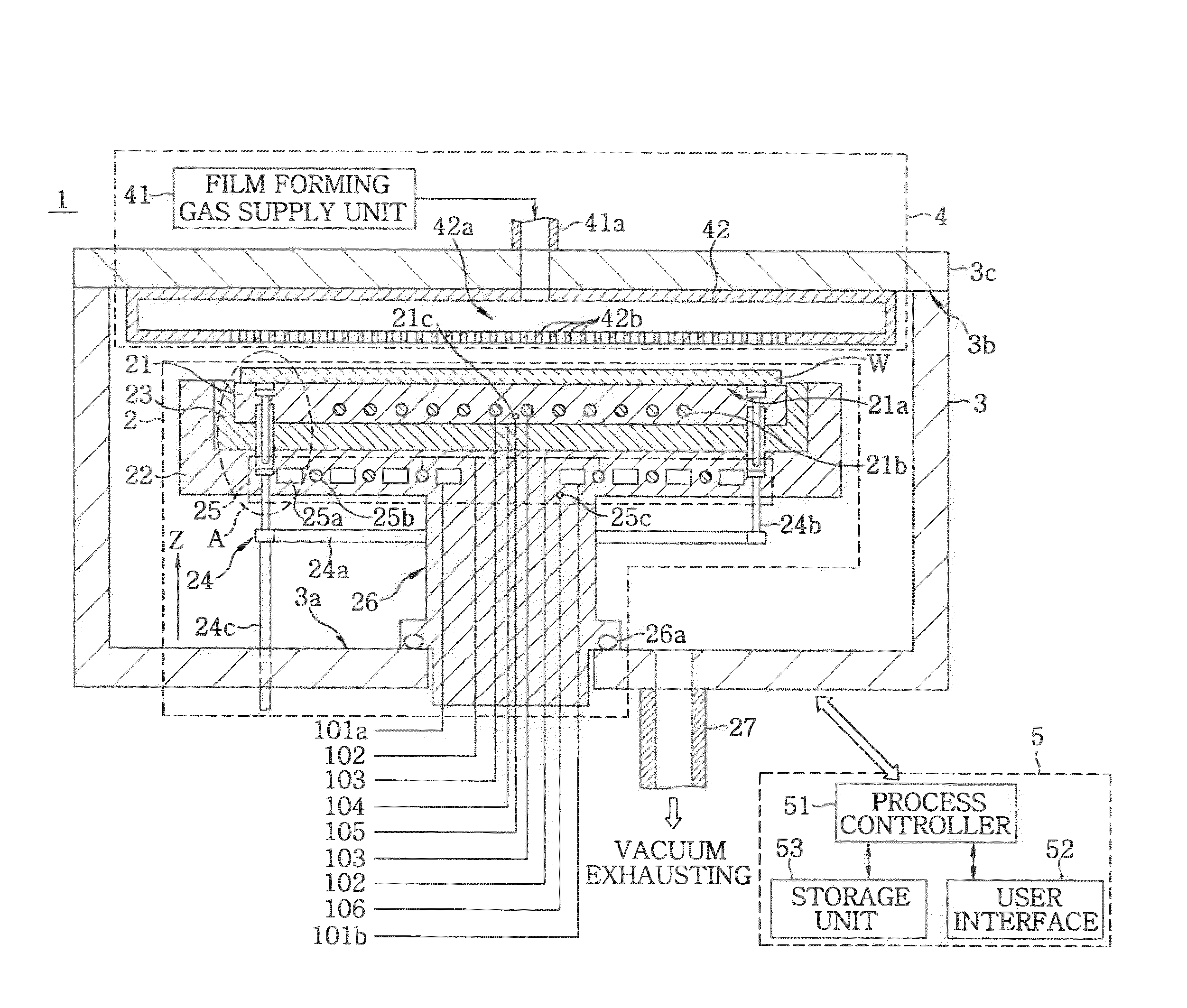
[0030]FIG. 1 is a cross sectional view schematically showing an example of a substrate processing apparatus in accordance with a first embodiment of the present invention.

[0031]As shown in FIG. 1, the substrate processing apparatus of the first embodiment is a CVD apparatus 1 for performing, e.g., a film forming process on a target substrate (in this embodiment, a semiconductor wafer) W. The CVD apparatus 1 includes a substrate mounting mechanism 2, a chamber 3 accommodating the substrate mounting mechanism 2, a film forming section 4 for performing a film forming process on a target substrate (in this embodiment, a semiconductor wafer) W, and a control section 5 for controlling the CVD apparatus 1.

[0032]The substrate mounting mechanism 2 includes a heater plate 21, a temperature control jacket 22, a thermal insulator 23 and a substrate lift mechanism 24.

[0033]The heater plate 21 has a substrate mounting surface 21a on which the target substrate is placed. A heater (hereinafter, ref...

second embodiment

[0088]FIG. 10 is a cross sectional view schematically showing an example of a substrate processing apparatus in accordance with a second embodiment of the present invention. In FIG. 10, the same reference numerals are given to the same components as those in FIG. 1, and only different features will be described.

[0089]As shown in FIG. 10, a CVD apparatus 1a of the second embodiment is different from the CVD apparatus 1 of the first embodiment in that the temperature control unit 25 is omitted from the temperature control jacket 22.

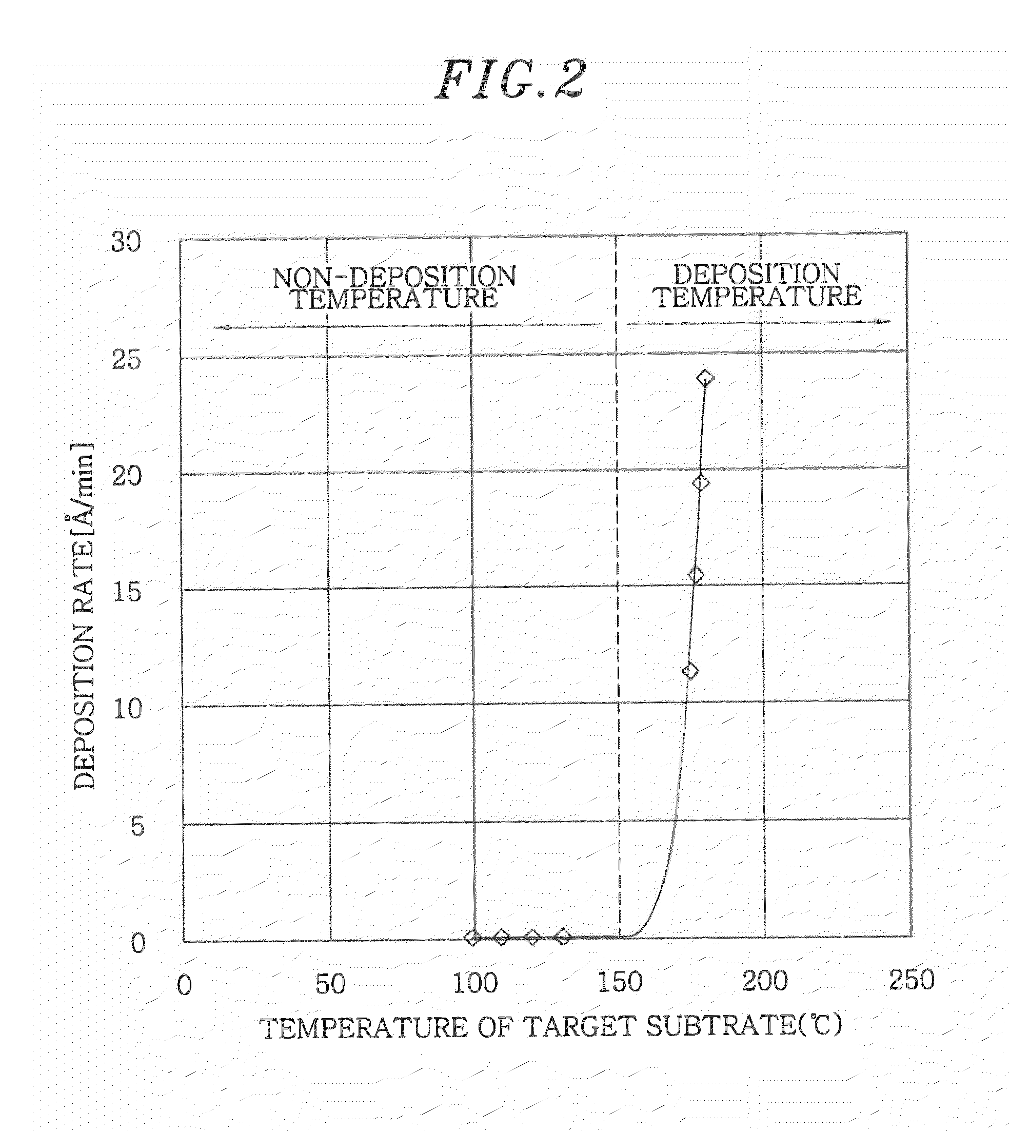
[0090]The thermal insulator 23 is interposed between the heater plate 21 and the temperature control jacket 22. The thermal insulator 23 suppresses heat transfer from the heater plate 21 to the temperature control jacket 22. Accordingly, even though the temperature control jacket 22 itself does not perform temperature control, the temperature of the temperature control jacket 22 can be set to have a non-deposition temperature lower than the temperature of t...

third embodiment

[0093]FIG. 11 is a cross sectional view schematically showing an example of a substrate processing apparatus in accordance with a third embodiment of the present invention. In FIG. 11, the same reference numerals are given to the same components as those in FIG. 1, and only different features will be described.

[0094]As shown in FIG. 11, a CVD apparatus 1b of the third embodiment is different from the CVD apparatus 1 of the first embodiment in that the thermal insulator 23 is omitted between the heater plate 21 and the temperature control jacket 22.

[0095]The temperature control jacket 22 of the CVD apparatus 1b has the temperature control unit 25 as in the first embodiment. In this case, the temperature of the temperature control jacket 22 can be adjusted to a non-deposition temperature without the thermal insulator 23. Accordingly, the thermal insulator 23 may be omitted if the temperature control jacket 22 has the temperature control unit 25.

[0096]In the third embodiment, the tempe...


PUM

PropertyMeasurementUnit
Temperatureaaaaaaaaaa
Diameteraaaaaaaaaa

Abstract

A substrate mounting mechanism on which a substrate is placed is provided. The mechanism includes a heater plate having a substrate mounting surface, and a first insertion hole having large and small diameter portions, and a temperature control jacket formed to cover at least a surface of the heater plate other than the substrate mounting surface and having a non-deposition temperature a second insertion hole having large and small diameter portions. The mechanism further includes a first lift pin having a cover inserted into the large diameter portion of the first insertion hole and a shaft inserted into both the large and small diameter portions of the first insertion hole, and a second lift pin having a cover to be inserted into the large diameter portion of the second insertion hole and a shaft to be inserted into both the large and small diameter portions of the second insertion hole.

Description

[0001]This application is a Continuation Application of PCT International Application No. PCT / JP2008 / 065877 filed on Sep. 3, 2008, which designated the United States.FIELD OF THE INVENTION[0002]The present invention relates to a substrate mounting mechanism having a heater to heat a substrate such as a semiconductor wafer mounted thereon in a processing chamber of a substrate processing apparatus such as a film forming apparatus, and a substrate processing apparatus including the substrate mounting mechanism.BACKGROUND OF THE INVENTION[0003]As one of manufacturing processes of semiconductor devices, there is a CVD film forming process that is performed on a semiconductor wafer serving as a target substrate. In this process, the semiconductor wafer serving as a target substrate is heated to a specific temperature generally by using a heater plate (stage heater) also serving as a substrate mounting table. A general heater plate is disclosed in Japanese Patent Application Publication N...

Claims


Application Information

Patent Timeline
IPC IPC(8): H01L21/46
CPCC23C16/4401C23C16/4586H01L21/68742H01L21/67103C23C16/46
Inventor HARA, MASAMICHIGOMI, ATSUSHIMAEKAWA, SHINJITAGA, SATOSHI
Owner TOKYO ELECTRON LTD
Why Eureka
Try Eureka