Method for fabricating carbon nanotube array sensor

a carbon nanotube array and sensor technology, applied in the field of sensors, can solve the problems of decreasing the sensitivity and precision of the carbon nanotube array sensor

Active Publication Date: 2010-08-26
TSINGHUA UNIV +1
View PDF10 Cites 4 Cited by
  • Summary
  • Abstract
  • Description
  • Claims
  • Application Information

AI Technical Summary

Problems solved by technology

Furthermore, the carbon nanotube array has no firm connection to the two electrodes because of bad wettability between the

Method used


Image

  • Method for fabricating carbon nanotube array sensor
  • Method for fabricating carbon nanotube array sensor
  • Method for fabricating carbon nanotube array sensor

Examples


Embodiment Construction

[0015]The disclosure is illustrated by way of example and not by way of limitation in the figures of the accompanying drawings in which like references indicate similar elements. It should be noted that references to “an” or “one” embodiment in this disclosure are not necessarily to the same embodiment, and such references mean at least one.

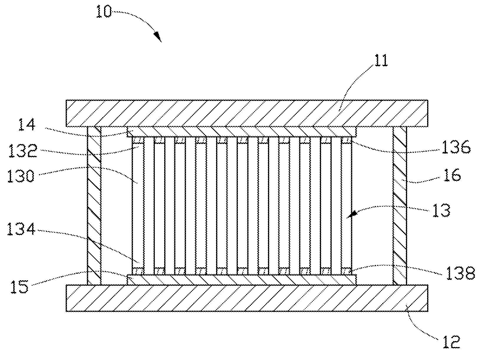
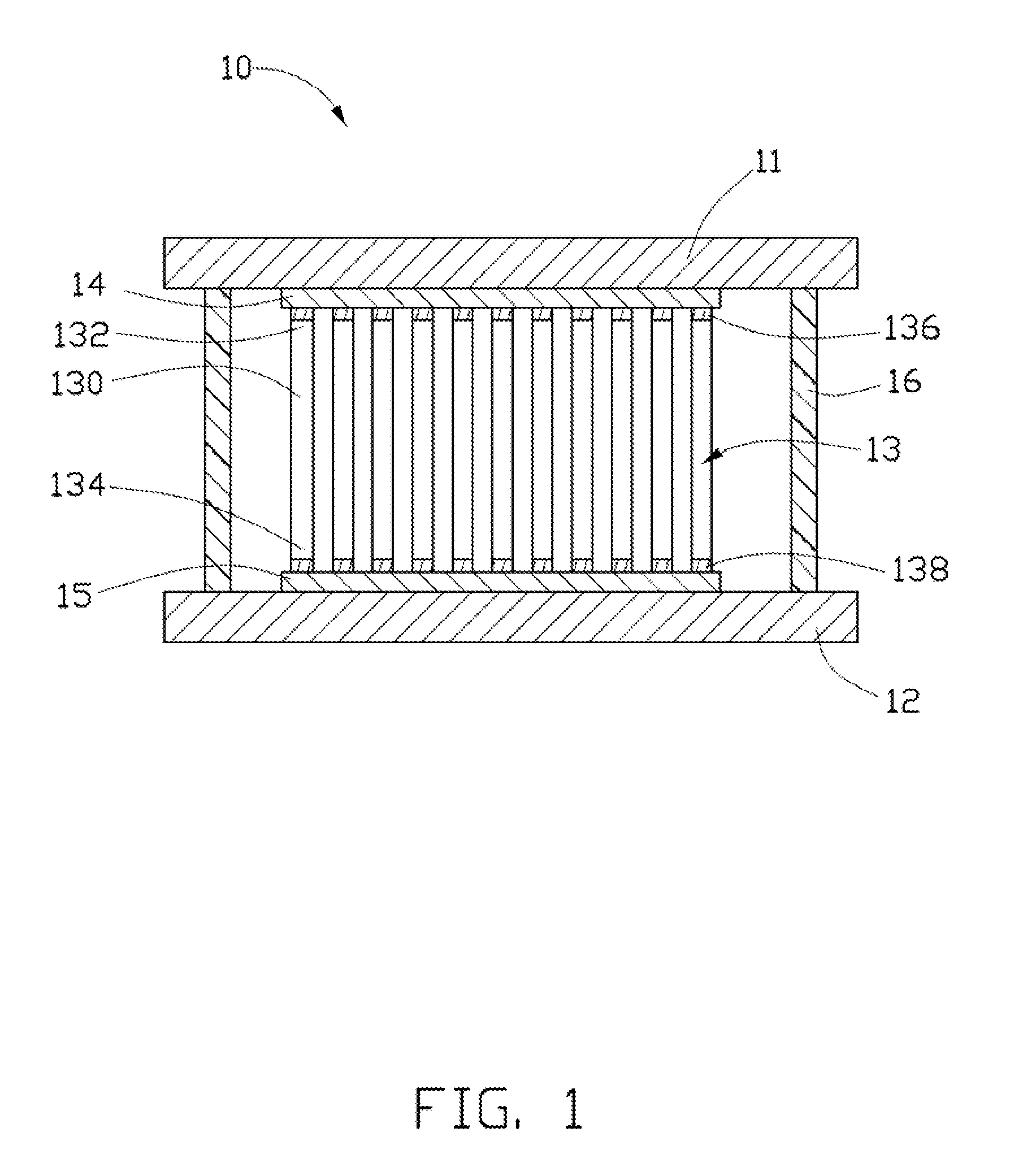
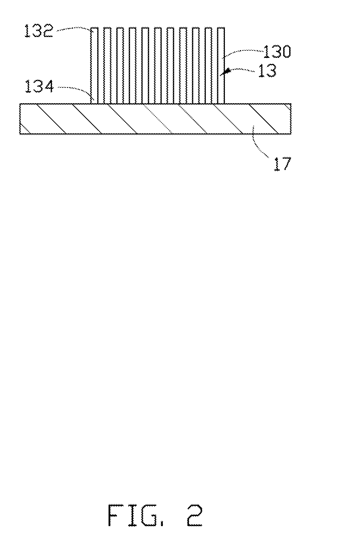
[0016]Referring to the embodiment shown FIG. 1, a carbon nanotube array sensor 10 includes a first electrode 11, a second electrode 12, a carbon nanotube array 13, a first conductive metal layer 14, and a second conductive metal layer 15. The carbon nanotube array 13 is located between the first and second electrodes 11, 12. The first conductive metal layer 14 is disposed between the first electrode 11 and the carbon nanotube array 13. The second conductive layer 15 is interposed between the second electrode 12 and the carbon nanotube array 13.

[0017]The first and second electrodes 11, 12 are spaced apart from each other and are made of conductive...


PUM


Abstract

A method of fabricating a carbon nanotube array sensor includes the following steps. A carbon nanotube array, a first electrode and a second electrode are provided, the carbon nanotube array includes a plurality of carbon nanotubes. Each of the carbon nanotubes includes a first end and a second end opposite to the first end. A first metallophilic layer is formed on the first end of each of the carbon nanotubes. At least one first conductive metal layer is arranged between the first metallophilic layer and the first electrode to electrically connect each of the carbon nanotubes with the first electrode. A second metallophilic layer is formed on the second end of each of the carbon nanotubes. At least one second conductive metal layer is arranged between the second metallophilic layer and the second electrode to electrically connect each of the carbon nanotubes with the second electrode.

Description

[0001]This application claims all benefits accruing under 35 U.S.C. §119 from China Patent Application No. 200910105489.8, filed on Feb. 20, 2009, in the China Intellectual Property Office. This application is a continuation application of U.S. patent application Ser. No. 12 / 570,621, filed Sep. 30, 2009, entitled, “carbon nanotube array sensor”.BACKGROUND[0002]1. Technical Field[0003]The present disclosure relates to sensors, and in particular, relates to a method for fabricating carbon nanotube array sensor.[0004]2. Description of the Related Art[0005]Carbon nanotubes can function as either a conductor, like metal, or a semiconductor, according to the rolled shape and the diameter of the helical tubes. With metallic-like nanotubes, it has been found that a one-dimensional carbon-based structure can conduct a current at room temperature with essentially no resistance. Further, electrons can be considered as moving freely through the structure, so that metallic-like nanotubes can be ...

Claims


Application Information

Patent Timeline
IPC IPC(8): H01L21/3205
CPCG01N27/414G01N27/127
Inventor YAO, YUAN
Owner TSINGHUA UNIV
Why Eureka
Try Eureka