Collector grid and interconnect structures for photovoltaic arrays and modules
a photovoltaic array and interconnection technology, applied in the field of photovoltaic array and interconnection structure, can solve the problems of high cost of single crystal silicon material and interconnection processing, thwarting the widespread energy collection of single-crystal silicon cells, and reducing the efficiency of photovoltaic energy collection, so as to achieve the effect of eliminating deficiencies
- Summary
- Abstract
- Description
- Claims
- Application Information
AI Technical Summary
Benefits of technology
Problems solved by technology
Method used
Image
Examples
example 1
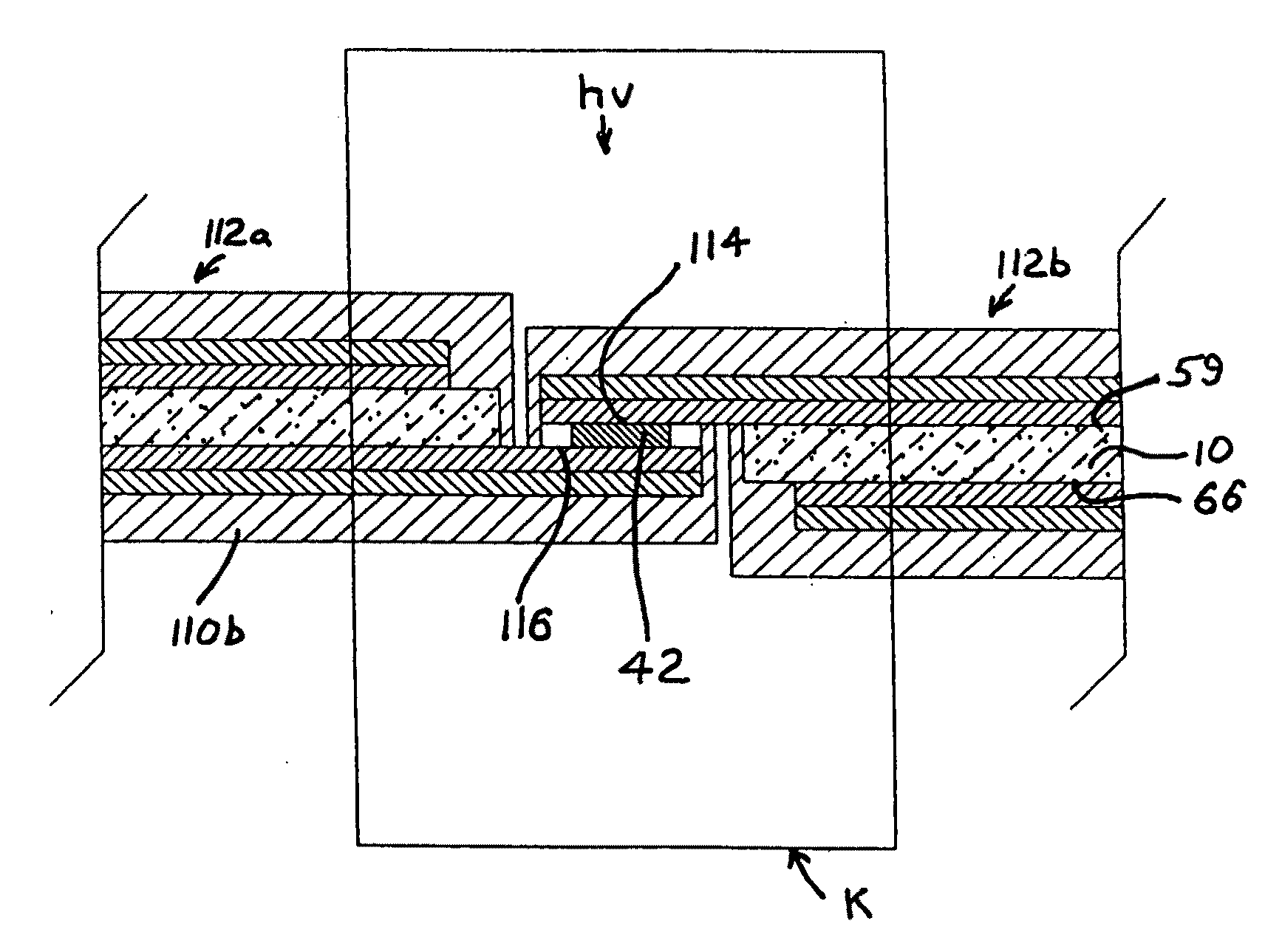
[0360]A standard plastic laminating sheet from GBC Corp. 75 micrometer (0.003 inch) thick was coated with DER in a pattern of repetitive fingers joined along one end with a busslike structure resulting in an article as embodied in FIGS. 16 through 19. The fingers were 0.020 inch wide, 1.625 inch long and were repetitively separated by 0.150 inch. The buss-like structure which contacted the fingers extended in a direction perpendicular to the fingers as shown in FIG. 16. The buss-like structure had a width of 0.25 inch. Both the finger pattern and buss-like structure were printed simultaneously using the same DER ink and using silk screen printing. The DER printing pattern was applied to the laminating sheet surface formed by the sealing layer (i.e. that surface facing to the inside of the standard sealing pouch).
[0361]The finger / buss pattern thus produced on the lamination sheet was then electroplated with nickel in a standard Watts nickel bath at a current density of 50 amps. per s...
example 2
[0365]Individual thin film CIGS semiconductor cells comprising a stainless steel supporting substrate 0.001 inch thick were cut to dimensions of 7.5 inch length and 1.75 inch width.
[0366]In a separate operation, multiple laminating collector grids were prepared as follows. A 0.002 inch thick film of Surlyn material was applied to both sides of a 0.003 inch thick PET film to produce a starting laminating substrate as embodied in FIG. 44. Holes having a 0.125 inch diameter were punched through the laminate to produce a structure as in FIG. 48. A DER ink was then printed on opposite surfaces and through the holes to form a pattern of DER traces. The resulting structure resembled that depicted in FIG. 51. The grid fingers 254 depicted in FIGS. 50 and 51 were 0.012 inch wide and 1.625 inch long and were spaced on centers 0.120 inch apart in the length direction. The grid fingers 252 were 0.062 inch wide and extended 1 inch and were spaced on centers 0.5 inch apart. The printed film was t...
PUM
 Abstract
Description
Claims
Application Information


