Light emitting module, backlight using the same, and liquid crystal display device
- Summary
- Abstract
- Description
- Claims
- Application Information
AI Technical Summary
Benefits of technology
Problems solved by technology
Method used
Image
Examples
examples 1 to 11
, and
Comparative Examples 1 to 2
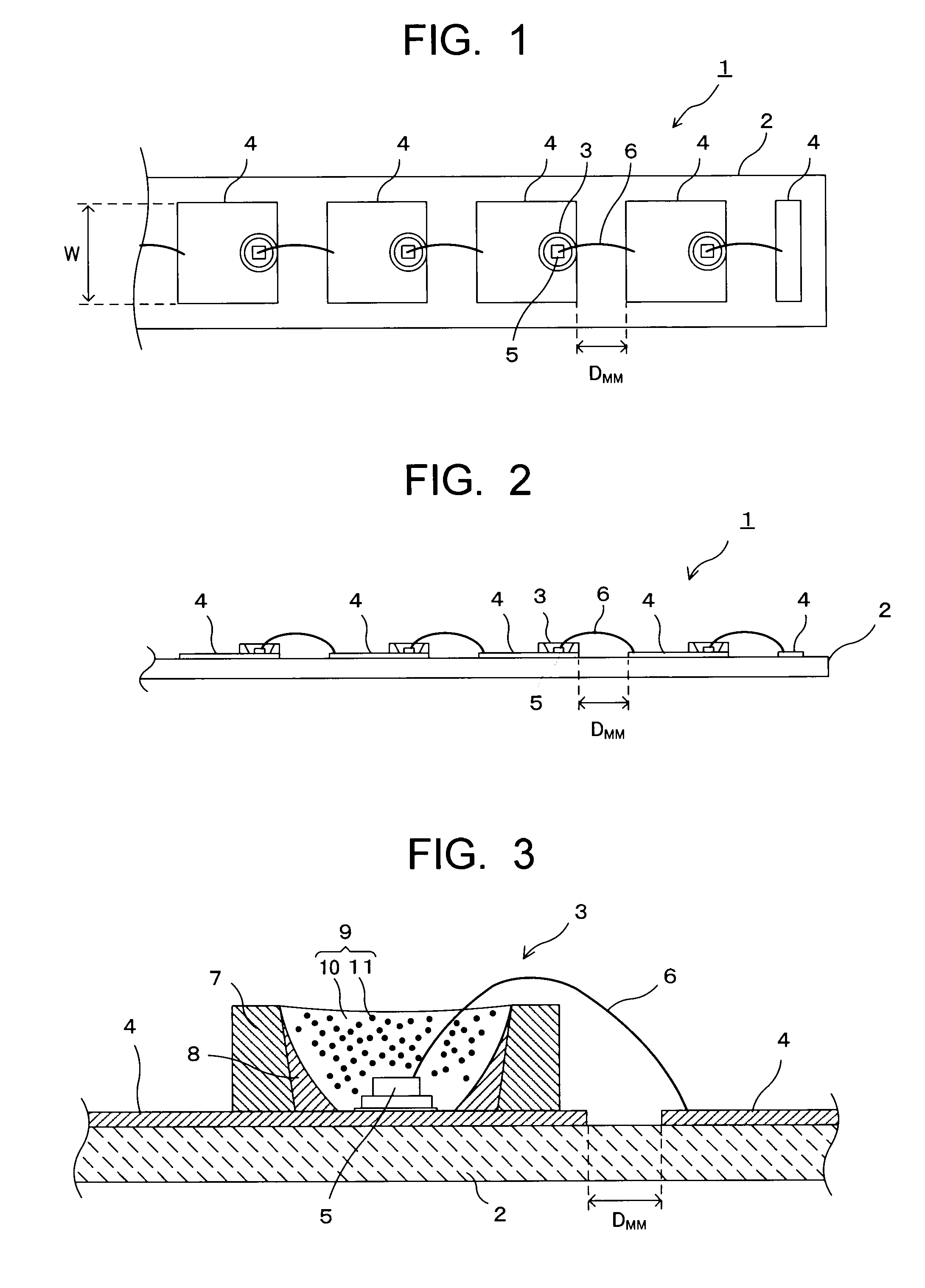
[0076]Here, the light emitting module 1 shown in FIG. 1 was manufactured. First, the plurality of quadrangular metal patterns 4 were formed on the substrate 2 having a length of 177 mm. The plurality of quadrangular metal patterns 4 are formed so that the LED chips 5 have predetermined linear densities when being mounted on the metal patterns 4. The size of the metal pattern 4 is controlled so that an area being a total sum of areas of the metal patterns 4 takes a predetermined area ratio with respect to the area of the substrate 2. Further, the surface roughness (arithmetic mean roughness Ra) of the metal pattern 4 is controlled to be in a predetermined range. The shape, and the like of the metal pattern 4 are as indicated as in Table 1.
[0077]Next, The LED chip 5 and the peripheral member 7 were bonded on the metal pattern 4, and further, the upper electrode of the LED chip 5 and the metal pattern 4 adjacent thereto were connected via a bonding wire ...
PUM
 Abstract
Description
Claims
Application Information


